Deck 6: BJT Amplifiers
ملء الشاشة (f)
سؤال
 Figure 4
Refer to Figure 4. The arrangement of transistors is called a
A)Sziklai pair
B)differential pair
C)Darlington pair
D)complementary follower
سؤال
سؤال
 Figure 7
Refer to Figure 7. Describe the expected signals at Vout1 and Vout2 with respect to the input
A)Vout1 is inverted; Vout2 is not- inverted
B)Vout1 is not- inverted; Vout2 is inverted
C)both are inverted
D)neither signal is inverted
سؤال
 Figure 2
Refer to Figure 2. The input resistance at the base, Rin(base), is approximately
A)12 k▲
B)8.5 k▲
C)17 k▲
D)5.8 k▲
سؤال
 Figure 3
Refer to Figure 3. Rin is approximately
A)1.0 k▲
B)1.8 k▲
C)4.5 k▲
D)2.7 k▲
سؤال
 Figure 6 Assume there is no loading effect of Q2/Q3 on Q1 and RL is the load.
Refer to Figure 6. The total voltage gain is approximately
A)75
B)100
C)25
D)50
سؤال
 Figure 5
Refer to Figure 5. Express the overall voltage gain as a standard voltage gain
A)100,000
B)1000
C)316
D)562
سؤال
 Figure 4
Refer to Figure 4. Assume each transistor has a fiac of 100. The overall fiac is
A)200
B)1,000
C)100
D)10,000
سؤال
سؤال
 Figure 7
Refer to Figure 7. Assume an identical signal is applied to input- 1 and input- 2 and further assume that RC1 = RC2. For this case, the ideal output is
A)zero
B)RC1/RE
C)RC1/2RE
D)twice the input
سؤال
سؤال
سؤال
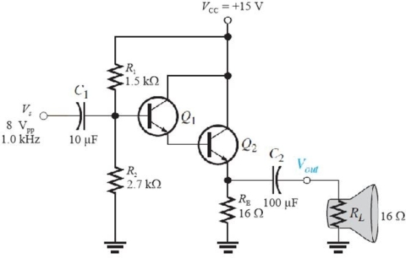 Figure 4
Refer to Figure 4. The input signal is an 8 Vpp sine wave driving a load that is a 16 ▲ speaker. The power delivered to the speaker is approximately
A)250 mW
B)0.75 W
C)1 W
D)0.5 W
سؤال
 Figure 6 Assume there is no loading effect of Q2/Q3 on Q1 and RL is the load.
Refer to Figure 6. Assume R2 is open. This would cause
A)no ac output
B)the dc voltage on Q1 base to decrease
C)an increase in IE1
D)all of the above
سؤال
 Figure 1
Refer to Figure 1. To calculate the input resistance looking in at Vin, you do not need to consider the value of
A)fiac
B)RC
C)RE
D)the bias resistors
سؤال
سؤال
 Figure 1
Refer to Figure 1. Looking in at Vin, the input resistance is approximately
A)5.6 k▲
B)14 k▲
C)39 k▲
D)1.8 k▲
سؤال
Figure 6 Assume there is no loading effect of Q2/Q3 on Q1 and RL is the load.Refer to Figure 6. The dc voltage across RL should be approximately
A)6.3 V
B)5.2 V
C)7.5 V
D)4.0 V
سؤال
 Figure 2
Refer to Figure 2. This circuit is an example of a
A)common- emitter amplifier
B)common- collector amplifier
C)common- base amplifier
D)none of the above
سؤال
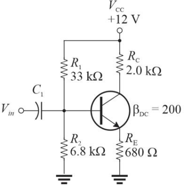 Figure 1
Refer to Figure 1. If a large capacitor is placed in parallel with RE, the input resistance will
A)increase
B)decrease
C)remain the same
سؤال
سؤال
 Figure 3
Refer to Figure 3. VE is approximately
A)1.0 V
B)5.0 V
C)2.5 V
D)7.5 V
سؤال
سؤال
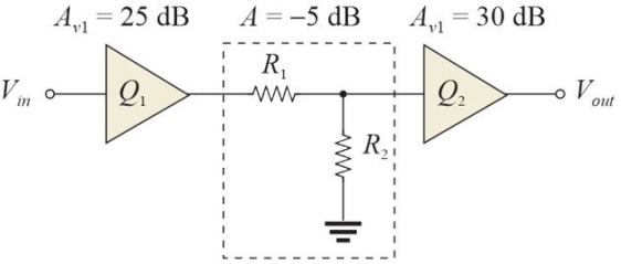 Figure 5
Refer to Figure 5. Explain the purpose of R1 and R2
A)R1 is the input resistance of Q2; R2 is the output resistance of Q1
B)R1 and R2 are the collector and emitter resistors of Q1
C)R1 is the output resistance of Q1; R2 is the input resistance of Q2
D)R1 and R2 are the bias resistors of Q2
سؤال
سؤال
 Figure 1
Refer to Figure 1. To calculate the input resistance looking in at Vin, dc sources are replaced with
A)the bias resistors
B)a ground
C)an open
D)the ac emitter resistance
سؤال
 Figure 3
Refer to Figure 3. The power delivered to RL is approximately
A)160 mW
B)360 mW
C)240 mW
D)80 mW
سؤال
سؤال
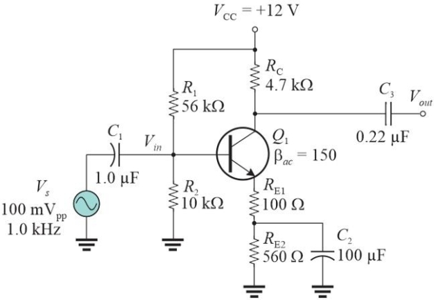 Figure 2
Refer to Figure 2. If RE1 and RE2 were switched, the
A)both the input resistance and the gain would increase
B)the input resistance would decrease and the gain would be unchanged
C)the input resistance would increase and the gain would decrease
D)IC would increase
سؤال
سؤال
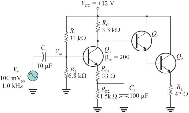 Figure 6 Assume there is no loading effect of Q2/Q3 on Q1 and RL is the load.
Refer to Figure 6. The input resistance is approximately
A)3.6 k▲
B)4.5 k▲
C)2.4 k▲
D)3.0 k▲
سؤال
سؤال
 Figure 2
Refer to Figure 2. The voltage gain is approximately
A)28
B)47
C)39
D)19
سؤال
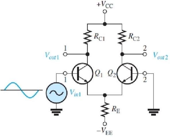 Figure 7
Refer to Figure 7. Assume output is taken between Vout1 and Vout2. This condition is a
A)double ended input with a differential output
B)differential input with a differential output
C)single ended input with a differential output
D)single ended input with a single ended output
سؤال
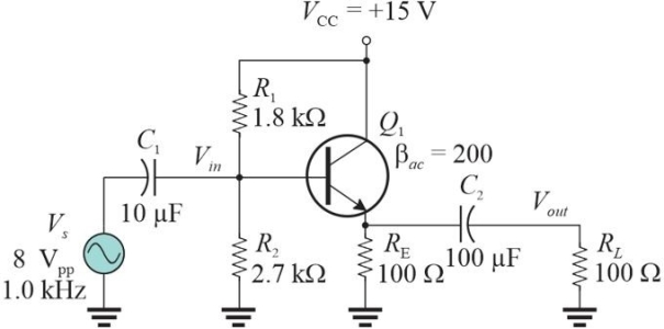 Figure 3
Refer to Figure 3. The power gain is approximately
A)5
B)20
C)40
D)10
سؤال
 Figure 5
Refer to Figure 5. The overall voltage gain of the amplifier in dB is
A)55 dB
B)50 dB
C)60 dB
D)none of the above
سؤال
سؤال
سؤال
 Figure 1
Refer to Figure 1. The ac emitter resistance, re', is approximately
A)680 ▲
B)8 ▲
C)13 ▲
D)25 ▲
سؤال
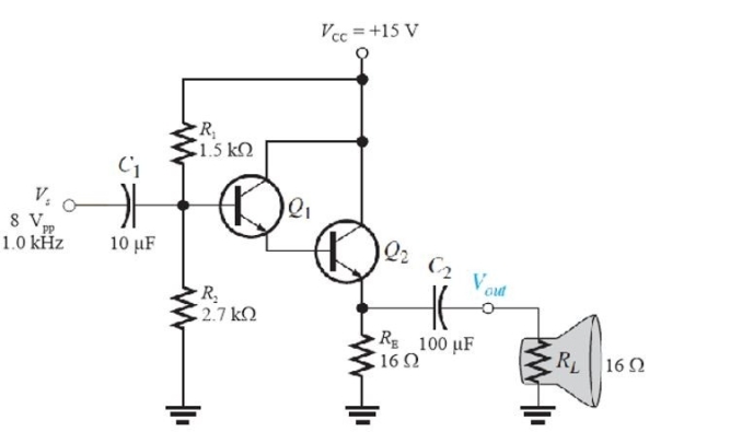 Figure 4
Compare Figure 4 to Figure 3. The two- transistor circuit in Figure 4 has
A)increased power gain
B)much more voltage gain
C)much higher input resistance
D)all of the above
سؤال
سؤال
سؤال

فتح الحزمة
قم بالتسجيل لفتح البطاقات في هذه المجموعة!
Unlock Deck
Unlock Deck
1/43
العب
ملء الشاشة (f)
Deck 6: BJT Amplifiers
1
Figure 4Refer to Figure 4. The arrangement of transistors is called a
A)Sziklai pair
B)differential pair
C)Darlington pair
D)complementary follower
C
2
The ac emitter resistance, re', is
A)is directly proportional to IE
B)generally measured with an ohmmeter
C)both A and B
D)none of the above
A)is directly proportional to IE
B)generally measured with an ohmmeter
C)both A and B
D)none of the above
D
3
Figure 7Refer to Figure 7. Describe the expected signals at Vout1 and Vout2 with respect to the input
A)Vout1 is inverted; Vout2 is not- inverted
B)Vout1 is not- inverted; Vout2 is inverted
C)both are inverted
D)neither signal is inverted
A
4
Figure 2Refer to Figure 2. The input resistance at the base, Rin(base), is approximately
A)12 k▲
B)8.5 k▲
C)17 k▲
D)5.8 k▲
فتح الحزمة
افتح القفل للوصول البطاقات البالغ عددها 43 في هذه المجموعة.
فتح الحزمة
k this deck
5
Figure 3Refer to Figure 3. Rin is approximately
A)1.0 k▲
B)1.8 k▲
C)4.5 k▲
D)2.7 k▲
فتح الحزمة
افتح القفل للوصول البطاقات البالغ عددها 43 في هذه المجموعة.
فتح الحزمة
k this deck
6
Figure 6 Assume there is no loading effect of Q2/Q3 on Q1 and RL is the load.Refer to Figure 6. The total voltage gain is approximately
A)75
B)100
C)25
D)50
فتح الحزمة
افتح القفل للوصول البطاقات البالغ عددها 43 في هذه المجموعة.
فتح الحزمة
k this deck
7
Figure 5Refer to Figure 5. Express the overall voltage gain as a standard voltage gain
A)100,000
B)1000
C)316
D)562
فتح الحزمة
افتح القفل للوصول البطاقات البالغ عددها 43 في هذه المجموعة.
فتح الحزمة
k this deck
8
Figure 4Refer to Figure 4. Assume each transistor has a fiac of 100. The overall fiac is
A)200
B)1,000
C)100
D)10,000
فتح الحزمة
افتح القفل للوصول البطاقات البالغ عددها 43 في هذه المجموعة.
فتح الحزمة
k this deck
9
The measurement unit for fiac is
A)the ohm
B)the volt
C)the ampere
D)there are no units as it is a ratio
A)the ohm
B)the volt
C)the ampere
D)there are no units as it is a ratio
فتح الحزمة
افتح القفل للوصول البطاقات البالغ عددها 43 في هذه المجموعة.
فتح الحزمة
k this deck
10
Figure 7Refer to Figure 7. Assume an identical signal is applied to input- 1 and input- 2 and further assume that RC1 = RC2. For this case, the ideal output is
A)zero
B)RC1/RE
C)RC1/2RE
D)twice the input
فتح الحزمة
افتح القفل للوصول البطاقات البالغ عددها 43 في هذه المجموعة.
فتح الحزمة
k this deck
11
In a common- base (CB)amplifier
A)open
B)connected through a large resistor to ground
C)the base lead is at dc ground
D)the base lead is at ac ground
A)open
B)connected through a large resistor to ground
C)the base lead is at dc ground
D)the base lead is at ac ground
فتح الحزمة
افتح القفل للوصول البطاقات البالغ عددها 43 في هذه المجموعة.
فتح الحزمة
k this deck
12
The hybrid parameter that is the same as fiac is
A)hrb
B)hfe
C)hrc
D)hoc
A)hrb
B)hfe
C)hrc
D)hoc
فتح الحزمة
افتح القفل للوصول البطاقات البالغ عددها 43 في هذه المجموعة.
فتح الحزمة
k this deck
13
Figure 4Refer to Figure 4. The input signal is an 8 Vpp sine wave driving a load that is a 16 ▲ speaker. The power delivered to the speaker is approximately
A)250 mW
B)0.75 W
C)1 W
D)0.5 W
فتح الحزمة
افتح القفل للوصول البطاقات البالغ عددها 43 في هذه المجموعة.
فتح الحزمة
k this deck
14
Figure 6 Assume there is no loading effect of Q2/Q3 on Q1 and RL is the load.Refer to Figure 6. Assume R2 is open. This would cause
A)no ac output
B)the dc voltage on Q1 base to decrease
C)an increase in IE1
D)all of the above
فتح الحزمة
افتح القفل للوصول البطاقات البالغ عددها 43 في هذه المجموعة.
فتح الحزمة
k this deck
15
Figure 1Refer to Figure 1. To calculate the input resistance looking in at Vin, you do not need to consider the value of
A)fiac
B)RC
C)RE
D)the bias resistors
فتح الحزمة
افتح القفل للوصول البطاقات البالغ عددها 43 في هذه المجموعة.
فتح الحزمة
k this deck
16
A CB amplifier has an advantage when you need
A)high input impedance
B)high frequency response with impedance matching
C)high current gain
D)all of the above
A)high input impedance
B)high frequency response with impedance matching
C)high current gain
D)all of the above
فتح الحزمة
افتح القفل للوصول البطاقات البالغ عددها 43 في هذه المجموعة.
فتح الحزمة
k this deck
17
Figure 1Refer to Figure 1. Looking in at Vin, the input resistance is approximately
A)5.6 k▲
B)14 k▲
C)39 k▲
D)1.8 k▲
فتح الحزمة
افتح القفل للوصول البطاقات البالغ عددها 43 في هذه المجموعة.
فتح الحزمة
k this deck
18
Figure 6 Assume there is no loading effect of Q2/Q3 on Q1 and RL is the load.Refer to Figure 6. The dc voltage across RL should be approximately
A)6.3 V
B)5.2 V
C)7.5 V
D)4.0 V
فتح الحزمة
افتح القفل للوصول البطاقات البالغ عددها 43 في هذه المجموعة.
فتح الحزمة
k this deck
19
Figure 2Refer to Figure 2. This circuit is an example of a
A)common- emitter amplifier
B)common- collector amplifier
C)common- base amplifier
D)none of the above
فتح الحزمة
افتح القفل للوصول البطاقات البالغ عددها 43 في هذه المجموعة.
فتح الحزمة
k this deck
20
Figure 1Refer to Figure 1. If a large capacitor is placed in parallel with RE, the input resistance will
A)increase
B)decrease
C)remain the same
فتح الحزمة
افتح القفل للوصول البطاقات البالغ عددها 43 في هذه المجموعة.
فتح الحزمة
k this deck
21
A typical common- base (CB)amplifier has
A)high current gain
B)high input resistance
C)high voltage gain
D)all of the above
A)high current gain
B)high input resistance
C)high voltage gain
D)all of the above
فتح الحزمة
افتح القفل للوصول البطاقات البالغ عددها 43 في هذه المجموعة.
فتح الحزمة
k this deck
22
Figure 3Refer to Figure 3. VE is approximately
A)1.0 V
B)5.0 V
C)2.5 V
D)7.5 V
فتح الحزمة
افتح القفل للوصول البطاقات البالغ عددها 43 في هذه المجموعة.
فتح الحزمة
k this deck
23
To calculate the end points for an ac load line, it is assumed that
A)the load resistor is removed
B)RC is in parallel with RE
C)ac and dc resistances are the same
D)capacitors are shorted
A)the load resistor is removed
B)RC is in parallel with RE
C)ac and dc resistances are the same
D)capacitors are shorted
فتح الحزمة
افتح القفل للوصول البطاقات البالغ عددها 43 في هذه المجموعة.
فتح الحزمة
k this deck
24
Figure 5Refer to Figure 5. Explain the purpose of R1 and R2
A)R1 is the input resistance of Q2; R2 is the output resistance of Q1
B)R1 and R2 are the collector and emitter resistors of Q1
C)R1 is the output resistance of Q1; R2 is the input resistance of Q2
D)R1 and R2 are the bias resistors of Q2
فتح الحزمة
افتح القفل للوصول البطاقات البالغ عددها 43 في هذه المجموعة.
فتح الحزمة
k this deck
25
Power gain can be found by multiplying current gain by the input resistance.
فتح الحزمة
افتح القفل للوصول البطاقات البالغ عددها 43 في هذه المجموعة.
فتح الحزمة
k this deck
26
Figure 1Refer to Figure 1. To calculate the input resistance looking in at Vin, dc sources are replaced with
A)the bias resistors
B)a ground
C)an open
D)the ac emitter resistance
فتح الحزمة
افتح القفل للوصول البطاقات البالغ عددها 43 في هذه المجموعة.
فتح الحزمة
k this deck
27
Figure 3Refer to Figure 3. The power delivered to RL is approximately
A)160 mW
B)360 mW
C)240 mW
D)80 mW
فتح الحزمة
افتح القفل للوصول البطاقات البالغ عددها 43 في هذه المجموعة.
فتح الحزمة
k this deck
28
In a CC amplifier, the power gain is approximately equal to the
A)voltage gain
B)current gain squared times RL
C)voltage gain squared divided by RL
D)current gain
A)voltage gain
B)current gain squared times RL
C)voltage gain squared divided by RL
D)current gain
فتح الحزمة
افتح القفل للوصول البطاقات البالغ عددها 43 في هذه المجموعة.
فتح الحزمة
k this deck
29
Figure 2Refer to Figure 2. If RE1 and RE2 were switched, the
A)both the input resistance and the gain would increase
B)the input resistance would decrease and the gain would be unchanged
C)the input resistance would increase and the gain would decrease
D)IC would increase
فتح الحزمة
افتح القفل للوصول البطاقات البالغ عددها 43 في هذه المجموعة.
فتح الحزمة
k this deck
30
An amplifier can invert the phase of a signal and still be a linear amplifier.
فتح الحزمة
افتح القفل للوصول البطاقات البالغ عددها 43 في هذه المجموعة.
فتح الحزمة
k this deck
31
Figure 6 Assume there is no loading effect of Q2/Q3 on Q1 and RL is the load.Refer to Figure 6. The input resistance is approximately
A)3.6 k▲
B)4.5 k▲
C)2.4 k▲
D)3.0 k▲
فتح الحزمة
افتح القفل للوصول البطاقات البالغ عددها 43 في هذه المجموعة.
فتح الحزمة
k this deck
32
A bypass capacitor normally should have high reactance.
فتح الحزمة
افتح القفل للوصول البطاقات البالغ عددها 43 في هذه المجموعة.
فتح الحزمة
k this deck
33
Figure 2Refer to Figure 2. The voltage gain is approximately
A)28
B)47
C)39
D)19
فتح الحزمة
افتح القفل للوصول البطاقات البالغ عددها 43 في هذه المجموعة.
فتح الحزمة
k this deck
34
Figure 7Refer to Figure 7. Assume output is taken between Vout1 and Vout2. This condition is a
A)double ended input with a differential output
B)differential input with a differential output
C)single ended input with a differential output
D)single ended input with a single ended output
فتح الحزمة
افتح القفل للوصول البطاقات البالغ عددها 43 في هذه المجموعة.
فتح الحزمة
k this deck
35
Figure 3Refer to Figure 3. The power gain is approximately
A)5
B)20
C)40
D)10
فتح الحزمة
افتح القفل للوصول البطاقات البالغ عددها 43 في هذه المجموعة.
فتح الحزمة
k this deck
36
Figure 5Refer to Figure 5. The overall voltage gain of the amplifier in dB is
A)55 dB
B)50 dB
C)60 dB
D)none of the above
فتح الحزمة
افتح القفل للوصول البطاقات البالغ عددها 43 في هذه المجموعة.
فتح الحزمة
k this deck
37
If a load resistor is connected to a CE amplifier, the gain will decrease.
فتح الحزمة
افتح القفل للوصول البطاقات البالغ عددها 43 في هذه المجموعة.
فتح الحزمة
k this deck
38
The Sziklai pair uses two types of transistors, an npn and a pnp.
فتح الحزمة
افتح القفل للوصول البطاقات البالغ عددها 43 في هذه المجموعة.
فتح الحزمة
k this deck
39
Figure 1Refer to Figure 1. The ac emitter resistance, re', is approximately
A)680 ▲
B)8 ▲
C)13 ▲
D)25 ▲
فتح الحزمة
افتح القفل للوصول البطاقات البالغ عددها 43 في هذه المجموعة.
فتح الحزمة
k this deck
40
Figure 4Compare Figure 4 to Figure 3. The two- transistor circuit in Figure 4 has
A)increased power gain
B)much more voltage gain
C)much higher input resistance
D)all of the above
فتح الحزمة
افتح القفل للوصول البطاقات البالغ عددها 43 في هذه المجموعة.
فتح الحزمة
k this deck
41
A differential amplifier should have a high common- mode rejection ratio.
فتح الحزمة
افتح القفل للوصول البطاقات البالغ عددها 43 في هذه المجموعة.
فتح الحزمة
k this deck
42
The power gain of a CC amplifier is approximately 1.
فتح الحزمة
افتح القفل للوصول البطاقات البالغ عددها 43 في هذه المجموعة.
فتح الحزمة
k this deck
43
The internal emitter resistance of a transistor is a dc resistance.
فتح الحزمة
افتح القفل للوصول البطاقات البالغ عددها 43 في هذه المجموعة.
فتح الحزمة
k this deck
فتح الحزمة
افتح القفل للوصول البطاقات البالغ عددها 43 في هذه المجموعة.


