Deck 12: Field-Effect Transistors
ملء الشاشة (f)
سؤال
سؤال
سؤال
سؤال
سؤال
سؤال
سؤال
سؤال
سؤال
سؤال
سؤال
سؤال
سؤال
سؤال
سؤال
سؤال
سؤال
سؤال
سؤال
سؤال
سؤال
The amplifier has low input impedance, high output impedance, and high voltage gain.
A) common-gate
B) common-drain
C) common-source
سؤال
The amplifier has high input impedance, low output impedance, and low-voltage gain.
A) common-gate
B) common-drain
C) common-source
سؤال
سؤال
سؤال
سؤال
The JFET in Figure has the following ratings: VGSoff) = -5 V and gm0 = 4000 μS. What is the value of Av for the circuit?
A) 1.2
B) 1.47
C) 0.4
D) 0.9
سؤال
The JFET in Figure has the following ratings: VGSoff) = -2 V to -10 V, gm0 = 1000 μS to 1600 μS. What is the approximate input impedance of the circuit?
A) 179 kΩ
B) 1 MΩ
C) 848 kΩ
D) 922 kΩ
سؤال
Assume that the JFET has values of IDSS = 12 mA and VGSoff) = -6 V. If VGG = -3 V, what is the value of ID for the circuit?
A) 1 mA
B) 3 mA
C) 4.55 mA
D) 6 mA
سؤال
سؤال
سؤال
سؤال

فتح الحزمة
قم بالتسجيل لفتح البطاقات في هذه المجموعة!
Unlock Deck
Unlock Deck
1/32
العب
ملء الشاشة (f)
Deck 12: Field-Effect Transistors
1
The terminal is the JFET counterpart of the BJT base terminal.
A) gate
B) drain
C) source
A) gate
B) drain
C) source
gate
2
JFETs are
A) current-controlled devices.
B) voltage-controlled devices.
C) frequency-controlled devices.
D) impedance-controlled devices.
A) current-controlled devices.
B) voltage-controlled devices.
C) frequency-controlled devices.
D) impedance-controlled devices.
voltage-controlled devices.
3
A JFET has the following ratings: VGSoff) = -2 V to -5 V and IDSS = 4 mA to 12 mA. The device is being used in a voltage divider circuit. When the load line is plotted, it is found that the VGS for the circuit has a range of -1 V to -3.5 V. What are the corresponding Qmax) values?
A) VGSQ = -1 V, IDQ = 7.68 mA
B) VGSQ = -3.5 V, IDQ = 1.1 mA
C) VGSQ = -1 V, IDQ = 1 mA
D) Cannot be determined with the information given.
A) VGSQ = -1 V, IDQ = 7.68 mA
B) VGSQ = -3.5 V, IDQ = 1.1 mA
C) VGSQ = -1 V, IDQ = 1 mA
D) Cannot be determined with the information given.
VGSQ = -3.5 V, IDQ = 1.1 mA
4
A JFET has values of IDSS = 12 mA and VGSoff) = -4 V. What is the value of ID at VGS = -8 V?
A) 12 mA
B) 0 mA
C) 4 mA
D) 2 mA
A) 12 mA
B) 0 mA
C) 4 mA
D) 2 mA
فتح الحزمة
افتح القفل للوصول البطاقات البالغ عددها 32 في هذه المجموعة.
فتح الحزمة
k this deck
5
The value of gm is always the value of gm0 for a given JFET.
A) less than
B) equal to
C) less than or equal to
D) greater than
A) less than
B) equal to
C) less than or equal to
D) greater than
فتح الحزمة
افتح القفل للوصول البطاقات البالغ عددها 32 في هذه المجموعة.
فتح الحزمة
k this deck
6
The region of the JFET drain curve that lies between pinchoff and breakdown is called
A) the constant-voltage region.
B) the ohmic region.
C) the constant-current region.
D) Both B and C above.
A) the constant-voltage region.
B) the ohmic region.
C) the constant-current region.
D) Both B and C above.
فتح الحزمة
افتح القفل للوصول البطاقات البالغ عددها 32 في هذه المجموعة.
فتح الحزمة
k this deck
7
A JFET has the following ratings: VGSoff) = -2 V to -5 V and IDSS = 4 mA to 12 mA. This device is being used in a self-bias circuit. When the bias line for the device is plotted, it is found that VGS for the circuit will have a range of -1 V to -2.5 V. What are the corresponding Qmin) values?
A) VGSQ = -1 V, IDQ = 1 mA
B) VGSQ = -2.5 V, IDQ = 250 μA
C) VGSQ = -1 V, IDQ = 7.86 mA
D) Cannot be determined with the information given.
A) VGSQ = -1 V, IDQ = 1 mA
B) VGSQ = -2.5 V, IDQ = 250 μA
C) VGSQ = -1 V, IDQ = 7.86 mA
D) Cannot be determined with the information given.
فتح الحزمة
افتح القفل للوصول البطاقات البالغ عددها 32 في هذه المجموعة.
فتح الحزمة
k this deck
8
The value of ID is always the value of IDSS for a given JFET.
A) less than
B) equal to
C) less than or equal to
D) greater than
A) less than
B) equal to
C) less than or equal to
D) greater than
فتح الحزمة
افتح القفل للوصول البطاقات البالغ عددها 32 في هذه المجموعة.
فتح الحزمة
k this deck
9
Which of the following is usually used to control the channel width of a given JFET?
A) VS
B) VGS
C) The operating frequency
D) ID
A) VS
B) VGS
C) The operating frequency
D) ID
فتح الحزمة
افتح القفل للوصول البطاقات البالغ عددها 32 في هذه المجموعة.
فتح الحزمة
k this deck
10
As the channel width of a JFET decreases, the source-to-drain resistance of the device
A) increases.
B) decreases.
A) increases.
B) decreases.
فتح الحزمة
افتح القفل للوصول البطاقات البالغ عددها 32 في هذه المجموعة.
فتح الحزمة
k this deck
11
A JFET has values of IDSS = 10 mA and VGSoff) = -5 V. What is the value of ID at VGS = -3 V?
A) 1.6 mA
B) 3.6 mA
C) 25.6 mA
D) 4 mA
A) 1.6 mA
B) 3.6 mA
C) 25.6 mA
D) 4 mA
فتح الحزمة
افتح القفل للوصول البطاقات البالغ عددها 32 في هذه المجموعة.
فتح الحزمة
k this deck
12
A JFET has the following ratings: VGSoff) = -2 V to -5 V and IDSS = 4 mA to 12 mA. The device is being used in a gate bias circuit with a gate supply voltage of VGG = -1 V. What is the difference between the minimum and maximum values of ID for the circuit?
A) 7.68 mA
B) 9.6 mA
C) 6.68 mA
D) 8.6 mA
A) 7.68 mA
B) 9.6 mA
C) 6.68 mA
D) 8.6 mA
فتح الحزمة
افتح القفل للوصول البطاقات البالغ عددها 32 في هذه المجموعة.
فتح الحزمة
k this deck
13
The value of VDS that causes ID to reach its maximum value at a constant value of VGS is called
A) VDmax).
B) pinchoff voltage.
C) VDSS.
D) None of these is correct.
A) VDmax).
B) pinchoff voltage.
C) VDSS.
D) None of these is correct.
فتح الحزمة
افتح القفل للوصول البطاقات البالغ عددها 32 في هذه المجموعة.
فتح الحزمة
k this deck
14
A given JFET has values of Vp = +10 V and IDSS = 8 mA. What is the value of VGSoff) for the device?
A) +10 V
B) -10 V
C) -5 V
D) Cannot be determined from the information given.
A) +10 V
B) -10 V
C) -5 V
D) Cannot be determined from the information given.
فتح الحزمة
افتح القفل للوصول البطاقات البالغ عددها 32 في هذه المجموعة.
فتح الحزمة
k this deck
15
Which of the JFET biasing circuits listed below provides the best Q-point stability?
A) Gate-bias
B) Self-bias
C) Voltage-divider bias
D) Current-source bias
A) Gate-bias
B) Self-bias
C) Voltage-divider bias
D) Current-source bias
فتح الحزمة
افتح القفل للوصول البطاقات البالغ عددها 32 في هذه المجموعة.
فتح الحزمة
k this deck
16
Which of the following statements is true?
A) JFET drain current is controlled by its input gate) current.
B) JFET channel width is controlled by its gate-source voltage.
C) There is only one way to vary JFET channel width.
D) JFET drain current at a given drain supply voltage) varies inversely with channel width.
A) JFET drain current is controlled by its input gate) current.
B) JFET channel width is controlled by its gate-source voltage.
C) There is only one way to vary JFET channel width.
D) JFET drain current at a given drain supply voltage) varies inversely with channel width.
فتح الحزمة
افتح القفل للوصول البطاقات البالغ عددها 32 في هذه المجموعة.
فتح الحزمة
k this deck
17
The terminal is the JFET counterpart of the BJT emitter terminal.
A) gate
B) drain
C) source
A) gate
B) drain
C) source
فتح الحزمة
افتح القفل للوصول البطاقات البالغ عددها 32 في هذه المجموعة.
فتح الحزمة
k this deck
18
A given JFET has values of gm0 = 1200 μS and VGSoff) = -4 V. What is the value of gm for the device at VGS = -2 V?
A) 600 μS
B) 1200 μS
C) 300 μS
D) Cannot be determined with the information given.
A) 600 μS
B) 1200 μS
C) 300 μS
D) Cannot be determined with the information given.
فتح الحزمة
افتح القفل للوصول البطاقات البالغ عددها 32 في هذه المجموعة.
فتح الحزمة
k this deck
19
The terminal is the JFET counterpart of the BJT collector terminal.
A) gate
B) drain
C) source
A) gate
B) drain
C) source
فتح الحزمة
افتح القفل للوصول البطاقات البالغ عددها 32 في هذه المجموعة.
فتح الحزمة
k this deck
20
The JFET uses a positive drain supply voltage VDD).
A) n-channel
B) p-channel
A) n-channel
B) p-channel
فتح الحزمة
افتح القفل للوصول البطاقات البالغ عددها 32 في هذه المجموعة.
فتح الحزمة
k this deck
21
The amplifier has low input impedance, high output impedance, and high voltage gain.
A) common-gate
B) common-drain
C) common-source
فتح الحزمة
افتح القفل للوصول البطاقات البالغ عددها 32 في هذه المجموعة.
فتح الحزمة
k this deck
22
The amplifier has high input impedance, low output impedance, and low-voltage gain.
A) common-gate
B) common-drain
C) common-source
فتح الحزمة
افتح القفل للوصول البطاقات البالغ عددها 32 في هذه المجموعة.
فتح الحزمة
k this deck
23
A given JFET has values of gm0 = 1200 μs and VGSoff) = -4 V. What is the approximate value of IDSS?
A) 4.8 mA
B) 9.6 mA
C) 2.4 mA
D) Cannot be determined with the information given.
A) 4.8 mA
B) 9.6 mA
C) 2.4 mA
D) Cannot be determined with the information given.
فتح الحزمة
افتح القفل للوصول البطاقات البالغ عددها 32 في هذه المجموعة.
فتح الحزمة
k this deck
24
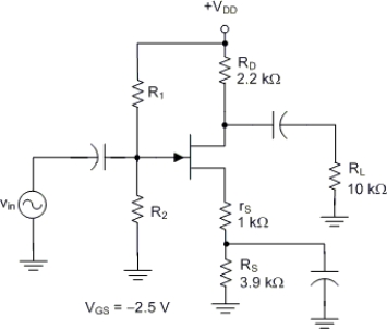
A given JFET has values of gm0 = 1000 μS and VGSoff) = -6 V. The device is being used in a common-source amplifier with values of RD = 2.2 kΩ, RL = 10 kΩ, and VGS = -1V. What is the value of Av for the circuit?
A) 1.5
B) 2.2
C) 10
D) Cannot be determined with the information given.
A) 1.5
B) 2.2
C) 10
D) Cannot be determined with the information given.
فتح الحزمة
افتح القفل للوصول البطاقات البالغ عددها 32 في هذه المجموعة.
فتح الحزمة
k this deck
25
In a JFET amplifier, VGS = -5 V, IG = 0 mA, and ID = IS = 5mA. Which of the following statements is true?
A) The gate terminal of the JFET is probably open.
B) The gate-source junction of the JFET is probably shorted.
C) The drain terminal of the JFET is probably open.
D) The readings do not indicate that any problem exists.
A) The gate terminal of the JFET is probably open.
B) The gate-source junction of the JFET is probably shorted.
C) The drain terminal of the JFET is probably open.
D) The readings do not indicate that any problem exists.
فتح الحزمة
افتح القفل للوصول البطاقات البالغ عددها 32 في هذه المجموعة.
فتح الحزمة
k this deck
26
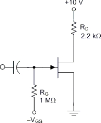
The JFET in Figure has the following ratings: VGSoff) = -5 V and gm0 = 4000 μS. What is the value of Av for the circuit?
A) 1.2
B) 1.47
C) 0.4
D) 0.9
فتح الحزمة
افتح القفل للوصول البطاقات البالغ عددها 32 في هذه المجموعة.
فتح الحزمة
k this deck
27
The JFET in Figure has the following ratings: VGSoff) = -2 V to -10 V, gm0 = 1000 μS to 1600 μS. What is the approximate input impedance of the circuit?
A) 179 kΩ
B) 1 MΩ
C) 848 kΩ
D) 922 kΩ
فتح الحزمة
افتح القفل للوصول البطاقات البالغ عددها 32 في هذه المجموعة.
فتح الحزمة
k this deck
28
Assume that the JFET has values of IDSS = 12 mA and VGSoff) = -6 V. If VGG = -3 V, what is the value of ID for the circuit?
A) 1 mA
B) 3 mA
C) 4.55 mA
D) 6 mA
فتح الحزمة
افتح القفل للوصول البطاقات البالغ عددها 32 في هذه المجموعة.
فتح الحزمة
k this deck
29
In a JFET amplifier, VGS = -2 V and ID = IDSS. Which of the following statements is true?
A) The gate terminal of the JFET is probably open.
B) The gate-source junction of the JFET is probably shorted.
C) The drain terminal of the JFET is probably open.
D) The readings do not indicate that any problem exists.
A) The gate terminal of the JFET is probably open.
B) The gate-source junction of the JFET is probably shorted.
C) The drain terminal of the JFET is probably open.
D) The readings do not indicate that any problem exists.
فتح الحزمة
افتح القفل للوصول البطاقات البالغ عددها 32 في هذه المجموعة.
فتح الحزمة
k this deck
30
Gate-source breakdown voltage can be defined as
A) the value gate-source voltage that will allow the channel to break down and conduct.
B) the value of gate-source voltage that will damage the JFET.
C) the maximum allowable value of VGS.
D) None of the above.
Chapter 12 Field-Effect Transistors Answer Key
A) the value gate-source voltage that will allow the channel to break down and conduct.
B) the value of gate-source voltage that will damage the JFET.
C) the maximum allowable value of VGS.
D) None of the above.
Chapter 12 Field-Effect Transistors Answer Key
فتح الحزمة
افتح القفل للوصول البطاقات البالغ عددها 32 في هذه المجموعة.
فتح الحزمة
k this deck
31
The high input impedance of a JFET amplifier prevents it from being used as a buffer.
فتح الحزمة
افتح القفل للوصول البطاقات البالغ عددها 32 في هذه المجموعة.
فتح الحزمة
k this deck
32
One advantage of using a JFET rf amplifier over a BJT amplifier is
A) high input impedance.
B) The JFET requires no signal input current.
C) The JFET is less susceptible to noise.
D) All of the above.
A) high input impedance.
B) The JFET requires no signal input current.
C) The JFET is less susceptible to noise.
D) All of the above.
فتح الحزمة
افتح القفل للوصول البطاقات البالغ عددها 32 في هذه المجموعة.
فتح الحزمة
k this deck
فتح الحزمة
افتح القفل للوصول البطاقات البالغ عددها 32 في هذه المجموعة.


