Deck 5: Differential and Multistage Amplifiers
ملء الشاشة (f)
سؤال
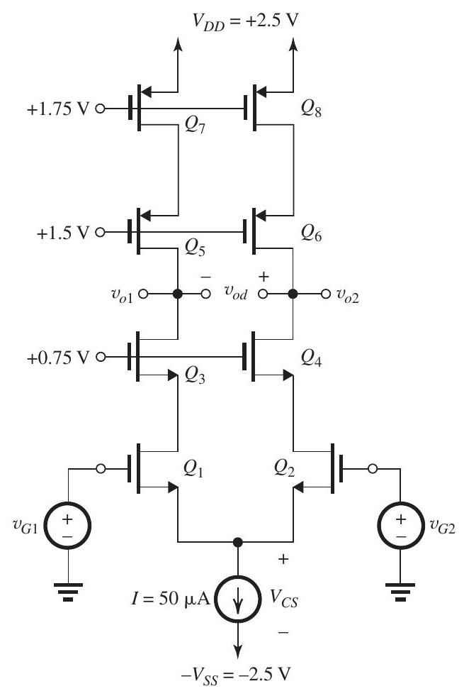
Figure 9.1.1
For the differential cascode amplifier in Fig. 9.1.1, all the transistors have the same threshold voltage and are operating at the same overdrive voltage. For the purpose of calculating dc quantities, neglect the Early effect. The current source requires a minimum dc voltage for its proper operation.
(a) With , find:
i. The bias current in each of the eight transistors.
ii. for each of the eight transistors. iii. for each transistor.
iv. and for each transistor assuming .
v. The dc voltage at the drains of and .
(b) Find the input common-mode range.
(c) With and , where , give the differential half-circuit and use it to determine the differential gain .
سؤال
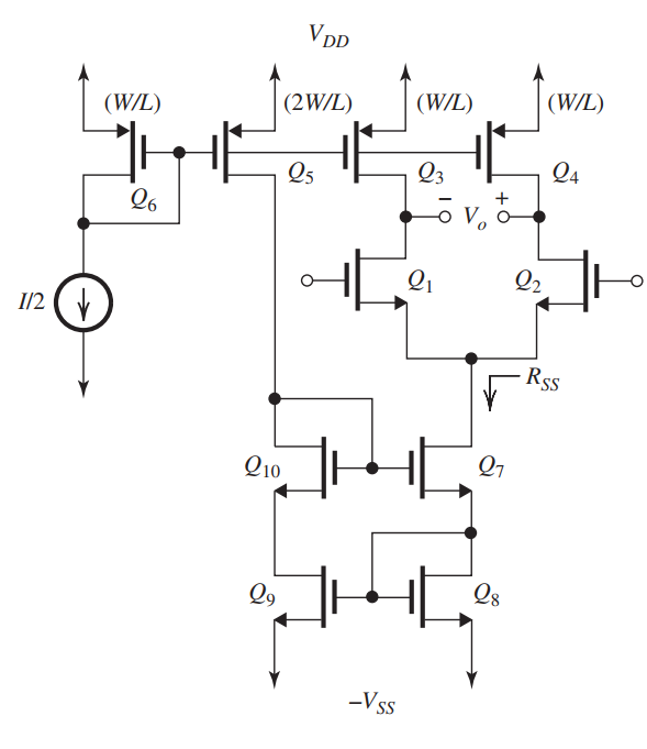
Figure 9.2.1
The differential amplifier in Fig. 9.2.1 utilizes current-source loads and is biased with a modified Wilson current mirror. All transistors are operated at the same overdrive voltage and have equal Early voltage, .
(a) Find the differential gain.
(b) Find the CMRR (in ) assuming that the
only mismatch is that between and with .
(c) If the Wilson mirror is replaced with a simple current mirror, what does the CMRR become?
سؤال
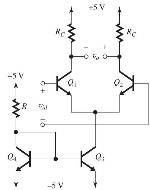
Figure 9.3.1
For the amplifier in Fig. 9.3.1:
(a) Assuming and have very high values, determine the value of that will provide a dc current of for each of and . (b) Assuming and have very high values, determine the value of that results in a dc voltage of at the collectors of and .
(c) What is the input common-mode range for this differential amplifier?
(d) Determine the value of the differential voltage gain .
(e) Determine the value of the input differential resistance, . Assume .
(f) If it is required to raise the value of by factor of 5 by including a resistance in the emitter of each of and , what value of is required? What is the resulting value of the differential gain?
(g) If the transistors have an Early voltage , calculate the worst-case value of the common-mode gain resulting from the resistances having finite tolerances of . Hence, find the value of the CMRR of the original amplifier (i.e., the one without the resistances included).
(h) With the two input terminals grounded, calculate the value of the worst-case differential dc voltage at the output resulting from the resistances having finite tolerances of . Hence, find the input offset voltage of the original amplifier (i.e., the one without 's).
سؤال
Figure 9.4.1
For the circuit shown in Fig. 9.4.1, neglect base currents in dc calculations and assume that for each transistor . Transistors and are perfectly matched. Transistor has twice the emitter-base junction area of .
(a) For , design the circuit to establish a dc bias current of in the collector of each of and and a dc voltage of at the collector of each of and . Specify the values required for , and .
(b) For and , determine the differential small-signal voltage gain . Ignore the Early effect. If , what is the differential input resistance of the differential amplifier ?
(c) If has an Early voltage of , find its output resistance and use this result to determine the common-mode gain of the differential amplifier , where and assuming that each of and is accurate to within . What is the resulting CMRR in decibels?
سؤال
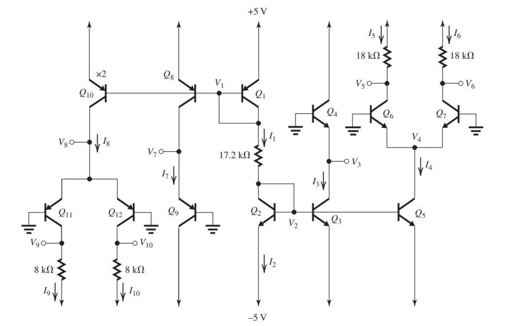
Figure 9.5.1
(a) For the circuit in Fig. 9.5.1 (refer to Figure above), assuming (i.e., ignoring base currents), and (i.e., ignoring the Early effect), find the dc values of the labelled currents and voltages.
(b) If the bases of and are disconnected from ground and a differential input signal is applied, find the differential gain if the output is taken between the two collectors.
(c) Repeat (b) for the differential amplifier .
سؤال
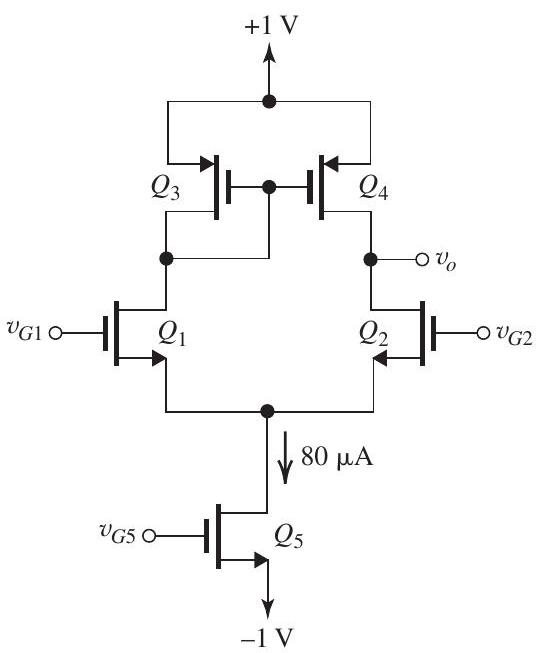
Figure 9.6.1
In the circuit of Fig. 9.6.1, all transistors are matched with , and .
(a) If , find the dc bias current in each of the four transistors , and , as well as the overdrive voltage for each. Ignore the Early effect. Also, find the de voltage at the sources of and , as well as the de voltage at the gates of and .
(b) Find of each of and , and determine of each of and .
(c) If and , find the differential gain .
(d) Find the output resistance of the biascurrent source and use it to determine the common mode gain in the case . Also, find the CMRR in .
(e) If it is required to increase the CMRR by , by what factor should the channel length of be changed?
سؤال
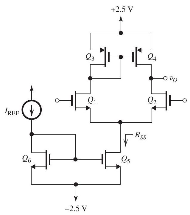
Figure 9.7.1
The current-mirror-loaded CMOS amplifier shown in Fig. 9.7.1 is fabricated in a technology for which , and . Transistors and are matched, and are matched, and and are matched. The ratios of all devices are selected so that all operate at the same .
(a) Starting from
and
show that
and
(b) To obtain a differential gain of , find the overdrive voltage at which the transistors should be operated. Also, find the resulting CMRR in .
(c) Using a reference current , find the required for each of the six transistors.
(d) With both input terminals grounded, what dc voltage occurs at the output (neglecting the Early effect)? Hence, compute the systematic input offset voltage.
(e) Find the input common-mode range.
(f) If the input differential signal is riding on an input common-mode voltage of , what is the maximum allowable output voltage swing in both directions? Hence, find the peak-to-peak amplitude of the largest sine-wave signal that can be applied between the two input terminals (without dc offset compensation).
سؤال
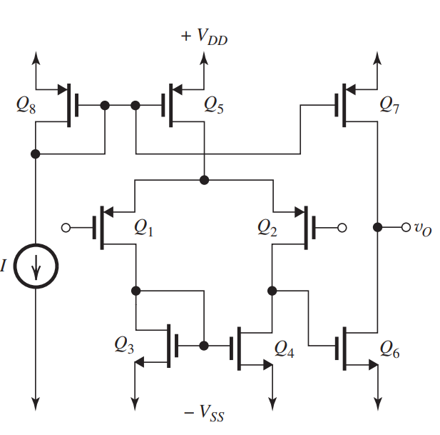
Figure 9.8.1
The two-stage CMOS op amp shown in Fig. 9.8.1 utilizes eight transistors, to , all having the same channel length . Transistors and are matched and and are matched. For the process technology utilized, . All transistors have the same Early voltage, .
(a) If the width of each of and is denoted , find the width of each of to in terms of so that all transistors operate at equal overdrive voltages, and that conducts a de bias current equal to that supplied by . Neglect the Early effect for this part.
(b) Derive an expression for the overall voltage gain in terms of and . Hence, determine the required value of for the case and the voltage gain required is .
سؤال
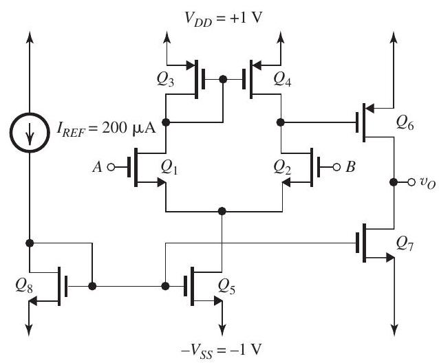
Figure 9.9.1
The two-stage CMOS op amp shown in Fig. 9.9.1 is fabricated in a technology having , and .
(a) With and grounded, perform a de design that will result in each of , and conducting a drain current of , and each of , and conducting a drain current of . Design so that all transistors operate at a overdrive voltage. Neglect the Early effect. Specify the ratio required for each MOSFET.
Present your results in a table. What is the dc voltage at the output (ideally)?
(b) Find the input common-mode range.
(c) Find the allowable range of the output voltage.
(d) With and , find the voltage gain . Assume that the Early voltage is .
سؤال
Refer to Figure 9.10.1 below.
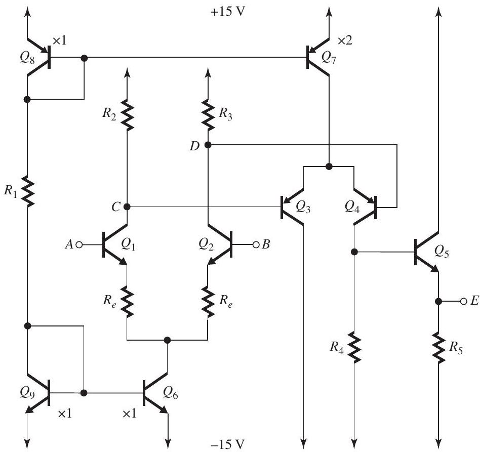
Figure 9.10.1
Note: Neglect the Early effect; that is, assume . Assume .
(a) For and neglecting all base currents, design the circuit of Fig. 9.10.1 so that each of and operates at a dc bias current of , and operates at a dc bias current of . Specify the dc bias current at which each of and will be operating and give the required value of , , and .
(b) If , what must the value of each of the two resistances labeled be so as to obtain an input differential resistance of ?
(c) Find the differential voltage gain of the input stage, .
(d) Find the voltage gain of the second stage, .
(e) Find the voltage gain of the output stage, .
(f) Find the overall voltage gain, .

فتح الحزمة
قم بالتسجيل لفتح البطاقات في هذه المجموعة!
Unlock Deck
Unlock Deck
1/10
العب
ملء الشاشة (f)
Deck 5: Differential and Multistage Amplifiers
1
Figure 9.1.1
For the differential cascode amplifier in Fig. 9.1.1, all the transistors have the same threshold voltage and are operating at the same overdrive voltage. For the purpose of calculating dc quantities, neglect the Early effect. The current source requires a minimum dc voltage for its proper operation.
(a) With , find:
i. The bias current in each of the eight transistors.
ii. for each of the eight transistors. iii. for each transistor.
iv. and for each transistor assuming .
v. The dc voltage at the drains of and .
(b) Find the input common-mode range.
(c) With and , where , give the differential half-circuit and use it to determine the differential gain .
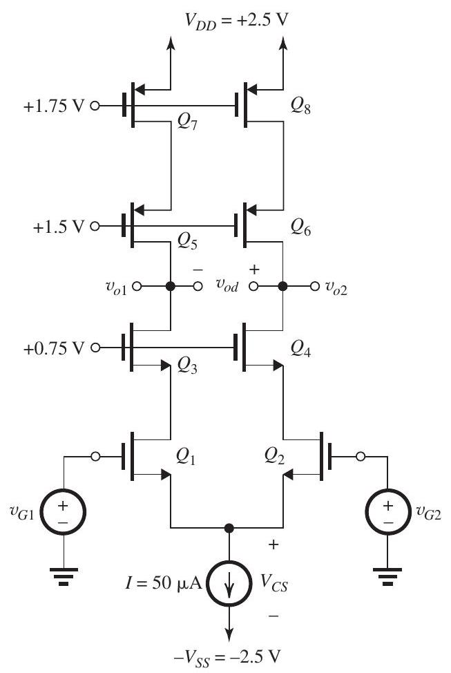
Figure 9.1.1
(a)
(i)
(ii) Since for and ,
and since all transistors have the same and , then
(iii)
(iv)
(v)
(b)
Thus,
(c)
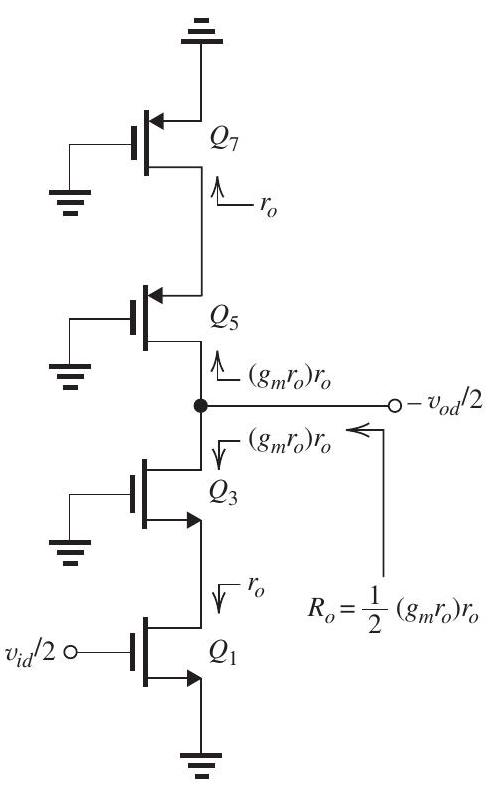
Figure 9.1.2
From the differential half-circuit in Fig. 9.1.2, we find
2
Figure 9.2.1
The differential amplifier in Fig. 9.2.1 utilizes current-source loads and is biased with a modified Wilson current mirror. All transistors are operated at the same overdrive voltage and have equal Early voltage, .
(a) Find the differential gain.
(b) Find the CMRR (in ) assuming that the
only mismatch is that between and with .
(c) If the Wilson mirror is replaced with a simple current mirror, what does the CMRR become?
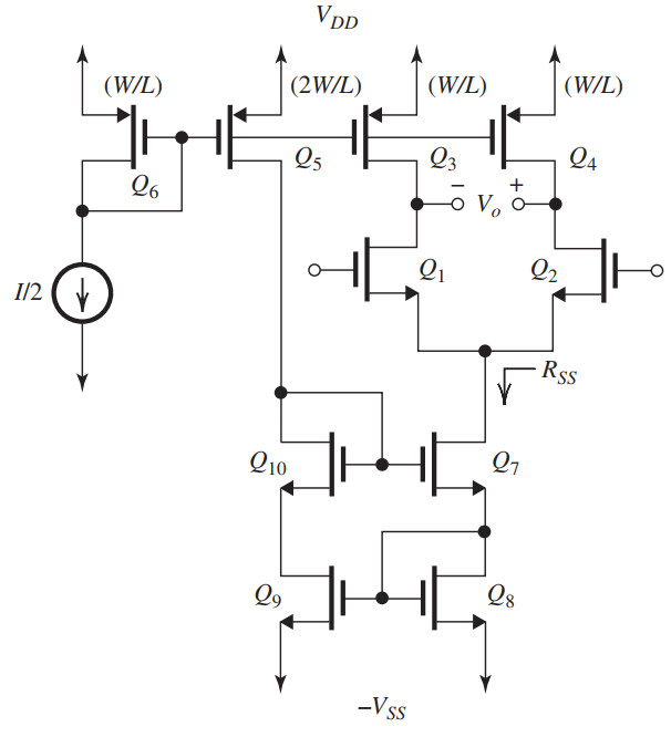
Figure 9.2.1 (a)
where
(b)
where
But
and
Thus,
or
(c) If the Wilson mirror is replaced with a simple current mirror,
Thus,
or
3
Figure 9.3.1
For the amplifier in Fig. 9.3.1:
(a) Assuming and have very high values, determine the value of that will provide a dc current of for each of and . (b) Assuming and have very high values, determine the value of that results in a dc voltage of at the collectors of and .
(c) What is the input common-mode range for this differential amplifier?
(d) Determine the value of the differential voltage gain .
(e) Determine the value of the input differential resistance, . Assume .
(f) If it is required to raise the value of by factor of 5 by including a resistance in the emitter of each of and , what value of is required? What is the resulting value of the differential gain?
(g) If the transistors have an Early voltage , calculate the worst-case value of the common-mode gain resulting from the resistances having finite tolerances of . Hence, find the value of the CMRR of the original amplifier (i.e., the one without the resistances included).
(h) With the two input terminals grounded, calculate the value of the worst-case differential dc voltage at the output resulting from the resistances having finite tolerances of . Hence, find the input offset voltage of the original amplifier (i.e., the one without 's).
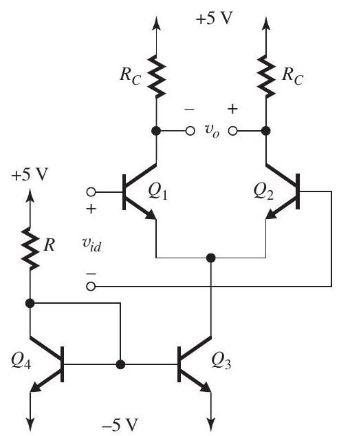
Figure 9.3.1
(a) To obtain a current in each of and , the current in must be . For and having high values, the current through and must be , thus
(b)
(c)
Thus,
(d)
where
Thus,
(e)
(f) To raise by a factor of 5 , we include a resistance in each of the emitters of and with given by
This will reduce the differential gain by the same factor of 5 , thus
(g)
where
Thus,
or .
(h)
4
Figure 9.4.1
For the circuit shown in Fig. 9.4.1, neglect base currents in dc calculations and assume that for each transistor . Transistors and are perfectly matched. Transistor has twice the emitter-base junction area of .
(a) For , design the circuit to establish a dc bias current of in the collector of each of and and a dc voltage of at the collector of each of and . Specify the values required for , and .
(b) For and , determine the differential small-signal voltage gain . Ignore the Early effect. If , what is the differential input resistance of the differential amplifier ?
(c) If has an Early voltage of , find its output resistance and use this result to determine the common-mode gain of the differential amplifier , where and assuming that each of and is accurate to within . What is the resulting CMRR in decibels?
فتح الحزمة
افتح القفل للوصول البطاقات البالغ عددها 10 في هذه المجموعة.
فتح الحزمة
k this deck
5
Figure 9.5.1
(a) For the circuit in Fig. 9.5.1 (refer to Figure above), assuming (i.e., ignoring base currents), and (i.e., ignoring the Early effect), find the dc values of the labelled currents and voltages.
(b) If the bases of and are disconnected from ground and a differential input signal is applied, find the differential gain if the output is taken between the two collectors.
(c) Repeat (b) for the differential amplifier .
فتح الحزمة
افتح القفل للوصول البطاقات البالغ عددها 10 في هذه المجموعة.
فتح الحزمة
k this deck
6
Figure 9.6.1
In the circuit of Fig. 9.6.1, all transistors are matched with , and .
(a) If , find the dc bias current in each of the four transistors , and , as well as the overdrive voltage for each. Ignore the Early effect. Also, find the de voltage at the sources of and , as well as the de voltage at the gates of and .
(b) Find of each of and , and determine of each of and .
(c) If and , find the differential gain .
(d) Find the output resistance of the biascurrent source and use it to determine the common mode gain in the case . Also, find the CMRR in .
(e) If it is required to increase the CMRR by , by what factor should the channel length of be changed?
فتح الحزمة
افتح القفل للوصول البطاقات البالغ عددها 10 في هذه المجموعة.
فتح الحزمة
k this deck
7
Figure 9.7.1
The current-mirror-loaded CMOS amplifier shown in Fig. 9.7.1 is fabricated in a technology for which , and . Transistors and are matched, and are matched, and and are matched. The ratios of all devices are selected so that all operate at the same .
(a) Starting from
and
show that
and
(b) To obtain a differential gain of , find the overdrive voltage at which the transistors should be operated. Also, find the resulting CMRR in .
(c) Using a reference current , find the required for each of the six transistors.
(d) With both input terminals grounded, what dc voltage occurs at the output (neglecting the Early effect)? Hence, compute the systematic input offset voltage.
(e) Find the input common-mode range.
(f) If the input differential signal is riding on an input common-mode voltage of , what is the maximum allowable output voltage swing in both directions? Hence, find the peak-to-peak amplitude of the largest sine-wave signal that can be applied between the two input terminals (without dc offset compensation).
فتح الحزمة
افتح القفل للوصول البطاقات البالغ عددها 10 في هذه المجموعة.
فتح الحزمة
k this deck
8
Figure 9.8.1
The two-stage CMOS op amp shown in Fig. 9.8.1 utilizes eight transistors, to , all having the same channel length . Transistors and are matched and and are matched. For the process technology utilized, . All transistors have the same Early voltage, .
(a) If the width of each of and is denoted , find the width of each of to in terms of so that all transistors operate at equal overdrive voltages, and that conducts a de bias current equal to that supplied by . Neglect the Early effect for this part.
(b) Derive an expression for the overall voltage gain in terms of and . Hence, determine the required value of for the case and the voltage gain required is .
فتح الحزمة
افتح القفل للوصول البطاقات البالغ عددها 10 في هذه المجموعة.
فتح الحزمة
k this deck
9
Figure 9.9.1
The two-stage CMOS op amp shown in Fig. 9.9.1 is fabricated in a technology having , and .
(a) With and grounded, perform a de design that will result in each of , and conducting a drain current of , and each of , and conducting a drain current of . Design so that all transistors operate at a overdrive voltage. Neglect the Early effect. Specify the ratio required for each MOSFET.
Present your results in a table. What is the dc voltage at the output (ideally)?
(b) Find the input common-mode range.
(c) Find the allowable range of the output voltage.
(d) With and , find the voltage gain . Assume that the Early voltage is .
فتح الحزمة
افتح القفل للوصول البطاقات البالغ عددها 10 في هذه المجموعة.
فتح الحزمة
k this deck
10
Refer to Figure 9.10.1 below.
Figure 9.10.1
Note: Neglect the Early effect; that is, assume . Assume .
(a) For and neglecting all base currents, design the circuit of Fig. 9.10.1 so that each of and operates at a dc bias current of , and operates at a dc bias current of . Specify the dc bias current at which each of and will be operating and give the required value of , , and .
(b) If , what must the value of each of the two resistances labeled be so as to obtain an input differential resistance of ?
(c) Find the differential voltage gain of the input stage, .
(d) Find the voltage gain of the second stage, .
(e) Find the voltage gain of the output stage, .
(f) Find the overall voltage gain, .
فتح الحزمة
افتح القفل للوصول البطاقات البالغ عددها 10 في هذه المجموعة.
فتح الحزمة
k this deck
فتح الحزمة
افتح القفل للوصول البطاقات البالغ عددها 10 في هذه المجموعة.


