Deck 7: BJT Biasing
ملء الشاشة (f)
سؤال
سؤال
سؤال
سؤال
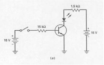
With the switch in the position as shown in Figure 7-4 (a),the LED is on.
سؤال
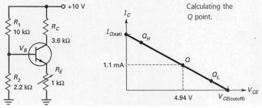
If RE is adjusted to its maximum value in Figure 7-16,the Q point moves toward saturation.
سؤال
سؤال
سؤال
سؤال
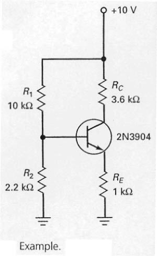
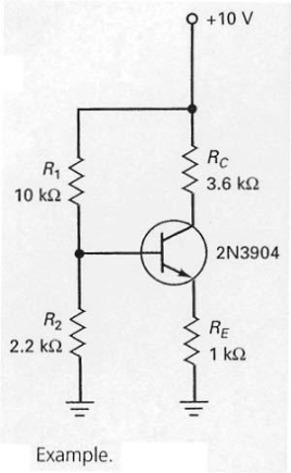
The emitter-base junction voltage of the silicon transistor shown in Figure 7-12 is approximated to be 0.3 V.
سؤال
In the circuit shown in Figure 7-26,if the base voltage measured 0 V and the emitter voltage measured 0 V,what should the troubleshooter do? 
A) replace the transistor
B) replace RE
C) check R1
D) check voltage source and leads
A) replace the transistor
B) replace RE
C) check R1
D) check voltage source and leads
سؤال
In the circuit shown in Figure 7-26,if R1 opens 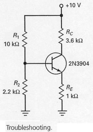
A) the collector voltage will be 10 V.
B) the collector voltage will be 0 V.
C) the base voltage will be 10 V.
D) the emitter voltage will be 10 V.
A) the collector voltage will be 10 V.
B) the collector voltage will be 0 V.
C) the base voltage will be 10 V.
D) the emitter voltage will be 10 V.
سؤال
In the circuit shown in Figure 7-12,the first step in finding the emitter current is to determine the voltage across R2.
سؤال
سؤال
سؤال
سؤال
Since voltage-divider bias is derived from emitter bias,the Q point is virtually immune to changes in current gain.

سؤال
سؤال
The emitter current in the circuit shown in Figure 7-12 can be calculated by dividing +10 V by 1 kW.

سؤال
If RE is adjusted it its minimum value in Figure 7-16,the Q point moves toward cut-off.

سؤال
سؤال
سؤال
سؤال
سؤال
سؤال
In Figure 7-18,the positive supply 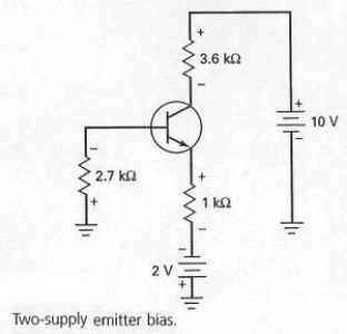
A) forward-biases the collector diode.
B) reverse-biases the collector diode.
C) forward-biases the emitter diode.
D) reverse-biases the emitter diode.
A) forward-biases the collector diode.
B) reverse-biases the collector diode.
C) forward-biases the emitter diode.
D) reverse-biases the emitter diode.
سؤال
In Figure 7-18,the negative supply 
A) forward-biases the emitter diode.
B) forward-biases the collector diode.
C) reverse-biases the emitter diode.
D) reverse-biases the collector diode.
A) forward-biases the emitter diode.
B) forward-biases the collector diode.
C) reverse-biases the emitter diode.
D) reverse-biases the collector diode.
سؤال
سؤال
While troubleshooting the circuit shown in Figure 7-26,the base voltage measures 1.8 V and the collector voltage measures 10 V,what should the technician do? 
A) replace the transistor
B) replace RE
C) check R1
D) check voltage source and leads
A) replace the transistor
B) replace RE
C) check R1
D) check voltage source and leads
سؤال
سؤال
سؤال
سؤال
سؤال
سؤال
In Figure 7-5,if the fuse blows open 
A) the transistor is biased on and the green LED illuminates.
B) the transistor is biased off and the green LED illuminates.
C) the transistor is biased on and the red LED illuminates.
D) the transistor is biased off and the red LED illuminates.
A) the transistor is biased on and the green LED illuminates.
B) the transistor is biased off and the green LED illuminates.
C) the transistor is biased on and the red LED illuminates.
D) the transistor is biased off and the red LED illuminates.
سؤال
The biasing configuration shown in Figure 7-18 is derived from emitter bias and is referred to as 
A) emitter derived bias (EDB).
B) bi-polar emitter bias (BPEB).
C) two-supply emitter bias (TSEB).
D) one-supply emitter bias (OSEB).
A) emitter derived bias (EDB).
B) bi-polar emitter bias (BPEB).
C) two-supply emitter bias (TSEB).
D) one-supply emitter bias (OSEB).
سؤال
In Figure 7-5,when the fuse is not blown 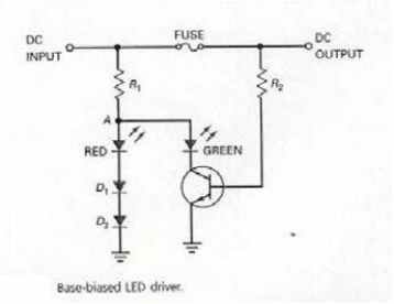
A) the transistor is biased on and the green LED illuminates.
B) the transistor is biased off and the green LED illuminates.
C) the transistor is biased on and the red LED illuminates.
D) the transistor is biased off and the red LED illuminates.
A) the transistor is biased on and the green LED illuminates.
B) the transistor is biased off and the green LED illuminates.
C) the transistor is biased on and the red LED illuminates.
D) the transistor is biased off and the red LED illuminates.
سؤال
سؤال
سؤال
سؤال
سؤال
The voltage measured across the base-emitter junction of the silicon transistor shown in Figure 7-29 (a)is ________. 
A) 0.3 V
B) 1.3 V
C) 0.7 V
D) 1.7 V
A) 0.3 V
B) 1.3 V
C) 0.7 V
D) 1.7 V
سؤال
In order to determine the emitter current for the circuit shown in Figure 7-21,you must 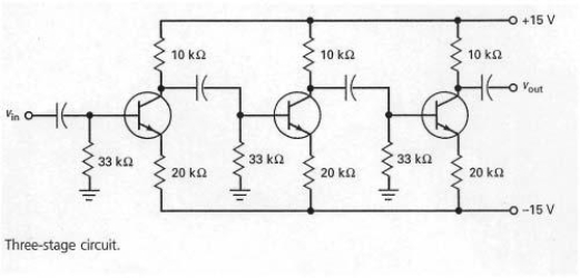
A) subtract 0.7 V from 15 V and then divide by 20 kW.
B) subtract 0.7 V from 15 V and then divide by 10 kW.
C) subtract 0.7 V from 15 V and then divide by 33 kW.
D) add 0.7 V to 15 V and then divide by 20 kW.
A) subtract 0.7 V from 15 V and then divide by 20 kW.
B) subtract 0.7 V from 15 V and then divide by 10 kW.
C) subtract 0.7 V from 15 V and then divide by 33 kW.
D) add 0.7 V to 15 V and then divide by 20 kW.
سؤال
سؤال
In Figure 7-21,what effect do the capacitors have on the bias voltage in each stage? 
A) increase
B) decrease
C) causes a cutoff condition
D) no effect
A) increase
B) decrease
C) causes a cutoff condition
D) no effect
سؤال
In order to calculate the base voltage for the circuit shown in Figure 7-29 (b) 
A) divide R2 by the sum of R1 and R2 and then multiply by 10 V.
B) divide R1 by the sum of R1 and R2 and then multiply by 10 V.
C) divide RC by the sum of RE and RC and then multiply by 10 V.
D) divide RE by the sum of RE and RC and then multiply by 10 V.
A) divide R2 by the sum of R1 and R2 and then multiply by 10 V.
B) divide R1 by the sum of R1 and R2 and then multiply by 10 V.
C) divide RC by the sum of RE and RC and then multiply by 10 V.
D) divide RE by the sum of RE and RC and then multiply by 10 V.
سؤال
سؤال
سؤال
Once the base voltage has been calculated for the circuit shown in Figure 7-29 (b),emitter voltage can be calculated by 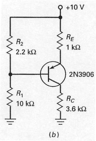
A) adding 0.7 V to the base voltage.
B) subtracting 0.7 V from the base voltage.
C) adding 0.3 V to the base voltage.
D) subtracting 0.3 V from the base voltage.
A) adding 0.7 V to the base voltage.
B) subtracting 0.7 V from the base voltage.
C) adding 0.3 V to the base voltage.
D) subtracting 0.3 V from the base voltage.
سؤال
In the circuit shown in Figure 7-29 (a),the base voltage can be calculated by 
A) using the voltage divider rule using R1 and R2 and the supply voltage.
B) using the voltage divider rule using RC and RE and the supply voltage.
C) multiplying collector current by the collector resistor.
D) multiplying emitter current by the emitter resistor.
A) using the voltage divider rule using R1 and R2 and the supply voltage.
B) using the voltage divider rule using RC and RE and the supply voltage.
C) multiplying collector current by the collector resistor.
D) multiplying emitter current by the emitter resistor.
سؤال

فتح الحزمة
قم بالتسجيل لفتح البطاقات في هذه المجموعة!
Unlock Deck
Unlock Deck
1/50
العب
ملء الشاشة (f)
Deck 7: BJT Biasing
1
Emitter bias is used to stabilize the Q point on the load line against current gain changes.
True
2
Collector-feedback bias is still sensitive to changes in current gain,but it is used because of its
A) small size.
B) low cost.
C) simplicity.
D) complexity.
A) small size.
B) low cost.
C) simplicity.
D) complexity.
C
3
A firm voltage divider means that the collector current will be approximately 10 percent lower than the stiff value.
True
4
With the switch in the position as shown in Figure 7-4 (a),the LED is on.
فتح الحزمة
افتح القفل للوصول البطاقات البالغ عددها 50 في هذه المجموعة.
فتح الحزمة
k this deck
5
If RE is adjusted to its maximum value in Figure 7-16,the Q point moves toward saturation.
فتح الحزمة
افتح القفل للوصول البطاقات البالغ عددها 50 في هذه المجموعة.
فتح الحزمة
k this deck
6
Emitter-feedback bias uses a resistor that provides negative feedback in attempt to stabilize the operating point.
فتح الحزمة
افتح القفل للوصول البطاقات البالغ عددها 50 في هذه المجموعة.
فتح الحزمة
k this deck
7
Emitter-feedback bias is also called self-bias.
فتح الحزمة
افتح القفل للوصول البطاقات البالغ عددها 50 في هذه المجموعة.
فتح الحزمة
k this deck
8
Emitter-feedback and collector-feedback are typically not adequate because
A) there is too much negative feedback.
B) there is not enough negative feedback.
C) circuitry is too complex.
D) there is not enough positive feedback.
A) there is too much negative feedback.
B) there is not enough negative feedback.
C) circuitry is too complex.
D) there is not enough positive feedback.
فتح الحزمة
افتح القفل للوصول البطاقات البالغ عددها 50 في هذه المجموعة.
فتح الحزمة
k this deck
9
The emitter-base junction voltage of the silicon transistor shown in Figure 7-12 is approximated to be 0.3 V.
فتح الحزمة
افتح القفل للوصول البطاقات البالغ عددها 50 في هذه المجموعة.
فتح الحزمة
k this deck
10
In the circuit shown in Figure 7-26,if the base voltage measured 0 V and the emitter voltage measured 0 V,what should the troubleshooter do?
A) replace the transistor
B) replace RE
C) check R1
D) check voltage source and leads
A) replace the transistor
B) replace RE
C) check R1
D) check voltage source and leads
فتح الحزمة
افتح القفل للوصول البطاقات البالغ عددها 50 في هذه المجموعة.
فتح الحزمة
k this deck
11
In the circuit shown in Figure 7-26,if R1 opens
A) the collector voltage will be 10 V.
B) the collector voltage will be 0 V.
C) the base voltage will be 10 V.
D) the emitter voltage will be 10 V.
A) the collector voltage will be 10 V.
B) the collector voltage will be 0 V.
C) the base voltage will be 10 V.
D) the emitter voltage will be 10 V.
فتح الحزمة
افتح القفل للوصول البطاقات البالغ عددها 50 في هذه المجموعة.
فتح الحزمة
k this deck
12
In the circuit shown in Figure 7-12,the first step in finding the emitter current is to determine the voltage across R2.
فتح الحزمة
افتح القفل للوصول البطاقات البالغ عددها 50 في هذه المجموعة.
فتح الحزمة
k this deck
13
Voltage-divider bias is really emitter bias in disguise.
فتح الحزمة
افتح القفل للوصول البطاقات البالغ عددها 50 في هذه المجموعة.
فتح الحزمة
k this deck
14
Collector-feedback bias is also called
A) self-bias.
B) collector follower.
C) negative collector.
D) voltage-divider.
A) self-bias.
B) collector follower.
C) negative collector.
D) voltage-divider.
فتح الحزمة
افتح القفل للوصول البطاقات البالغ عددها 50 في هذه المجموعة.
فتح الحزمة
k this deck
15
A well-designed voltage-divider bias circuit is one in which the voltage divider appears stiff to the input resistance of the base.
فتح الحزمة
افتح القفل للوصول البطاقات البالغ عددها 50 في هذه المجموعة.
فتح الحزمة
k this deck
16
Since voltage-divider bias is derived from emitter bias,the Q point is virtually immune to changes in current gain.
فتح الحزمة
افتح القفل للوصول البطاقات البالغ عددها 50 في هذه المجموعة.
فتح الحزمة
k this deck
17
Some electronic equipment has a power supply that produces both positive and negative supply voltages.
فتح الحزمة
افتح القفل للوصول البطاقات البالغ عددها 50 في هذه المجموعة.
فتح الحزمة
k this deck
18
The emitter current in the circuit shown in Figure 7-12 can be calculated by dividing +10 V by 1 kW.
فتح الحزمة
افتح القفل للوصول البطاقات البالغ عددها 50 في هذه المجموعة.
فتح الحزمة
k this deck
19
If RE is adjusted it its minimum value in Figure 7-16,the Q point moves toward cut-off.
فتح الحزمة
افتح القفل للوصول البطاقات البالغ عددها 50 في هذه المجموعة.
فتح الحزمة
k this deck
20
With the values shown at the operating point labeled Q,the voltage across RC would be 10 V.
فتح الحزمة
افتح القفل للوصول البطاقات البالغ عددها 50 في هذه المجموعة.
فتح الحزمة
k this deck
21
A well-designed voltage-divider bias circuit is one in which the voltage divider appears
A) stiff to the input resistance of the base.
B) soft to the input resistance of the base.
C) stiff to the output resistance of the collector.
D) stiff to the input resistance of the emitter.
A) stiff to the input resistance of the base.
B) soft to the input resistance of the base.
C) stiff to the output resistance of the collector.
D) stiff to the input resistance of the emitter.
فتح الحزمة
افتح القفل للوصول البطاقات البالغ عددها 50 في هذه المجموعة.
فتح الحزمة
k this deck
22
To prevent meter loading,a voltmeter used to make transistor circuit voltage measurements should have an input impedance of ________.
A) 10 kW
B) 100 kW
C) 1 MW
D) 10 MW
A) 10 kW
B) 100 kW
C) 1 MW
D) 10 MW
فتح الحزمة
افتح القفل للوصول البطاقات البالغ عددها 50 في هذه المجموعة.
فتح الحزمة
k this deck
23
Collector-feedback bias is also called
A) collector-follower bias.
B) emitter-feedback bias.
C) voltage-divider bias.
D) self-bias.
A) collector-follower bias.
B) emitter-feedback bias.
C) voltage-divider bias.
D) self-bias.
فتح الحزمة
افتح القفل للوصول البطاقات البالغ عددها 50 في هذه المجموعة.
فتح الحزمة
k this deck
24
What type transistor is used when the electronics equipment has a negative power supply?
A) field effect
B) small-signal
C) npn
D) pnp
A) field effect
B) small-signal
C) npn
D) pnp
فتح الحزمة
افتح القفل للوصول البطاقات البالغ عددها 50 في هذه المجموعة.
فتح الحزمة
k this deck
25
In Figure 7-18,the positive supply
A) forward-biases the collector diode.
B) reverse-biases the collector diode.
C) forward-biases the emitter diode.
D) reverse-biases the emitter diode.
A) forward-biases the collector diode.
B) reverse-biases the collector diode.
C) forward-biases the emitter diode.
D) reverse-biases the emitter diode.
فتح الحزمة
افتح القفل للوصول البطاقات البالغ عددها 50 في هذه المجموعة.
فتح الحزمة
k this deck
26
In Figure 7-18,the negative supply
A) forward-biases the emitter diode.
B) forward-biases the collector diode.
C) reverse-biases the emitter diode.
D) reverse-biases the collector diode.
A) forward-biases the emitter diode.
B) forward-biases the collector diode.
C) reverse-biases the emitter diode.
D) reverse-biases the collector diode.
فتح الحزمة
افتح القفل للوصول البطاقات البالغ عددها 50 في هذه المجموعة.
فتح الحزمة
k this deck
27
The intent of emitter-feedback bias is to
A) reduce the source voltage.
B) swamp out the variations in current gain.
C) swamp out the base current.
D) increase current gain.
A) reduce the source voltage.
B) swamp out the variations in current gain.
C) swamp out the base current.
D) increase current gain.
فتح الحزمة
افتح القفل للوصول البطاقات البالغ عددها 50 في هذه المجموعة.
فتح الحزمة
k this deck
28
While troubleshooting the circuit shown in Figure 7-26,the base voltage measures 1.8 V and the collector voltage measures 10 V,what should the technician do?
A) replace the transistor
B) replace RE
C) check R1
D) check voltage source and leads
A) replace the transistor
B) replace RE
C) check R1
D) check voltage source and leads
فتح الحزمة
افتح القفل للوصول البطاقات البالغ عددها 50 في هذه المجموعة.
فتح الحزمة
k this deck
29
By exposing a transistor's collector junction to light,a manufacturer can produce
A) an LED.
B) a seven-segment display.
C) a common-emitter circuit.
D) a phototransistor.
A) an LED.
B) a seven-segment display.
C) a common-emitter circuit.
D) a phototransistor.
فتح الحزمة
افتح القفل للوصول البطاقات البالغ عددها 50 في هذه المجموعة.
فتح الحزمة
k this deck
30
Using a firm voltage divider means that the collector current will be approximately
A) 5 percent lower than the stiff value.
B) 10 percent lower than the stiff value.
C) 50 percent lower than the stiff value.
D) 10 percent higher than the stiff value.
A) 5 percent lower than the stiff value.
B) 10 percent lower than the stiff value.
C) 50 percent lower than the stiff value.
D) 10 percent higher than the stiff value.
فتح الحزمة
افتح القفل للوصول البطاقات البالغ عددها 50 في هذه المجموعة.
فتح الحزمة
k this deck
31
The most widely used transistor biasing circuit is called
A) negative bias.
B) voltage-multiplier bias.
C) voltage-divider bias.
D) full-wave bridge bias.
A) negative bias.
B) voltage-multiplier bias.
C) voltage-divider bias.
D) full-wave bridge bias.
فتح الحزمة
افتح القفل للوصول البطاقات البالغ عددها 50 في هذه المجموعة.
فتح الحزمة
k this deck
32
Emitter-feedback and collector-feedback bias circuits are inadequate because
A) there is not enough negative feedback.
B) there is too much negative feedback.
C) circuits are too complex.
D) there is not enough positive feedback.
A) there is not enough negative feedback.
B) there is too much negative feedback.
C) circuits are too complex.
D) there is not enough positive feedback.
فتح الحزمة
افتح القفل للوصول البطاقات البالغ عددها 50 في هذه المجموعة.
فتح الحزمة
k this deck
33
Emitter-feedback bias has never become popular because the movement of the Q point is
A) stationary at cutoff.
B) stationary at saturation.
C) too large for applications that must be mass-produced.
D) too small for applications that must be mass-produced.
A) stationary at cutoff.
B) stationary at saturation.
C) too large for applications that must be mass-produced.
D) too small for applications that must be mass-produced.
فتح الحزمة
افتح القفل للوصول البطاقات البالغ عددها 50 في هذه المجموعة.
فتح الحزمة
k this deck
34
In Figure 7-5,if the fuse blows open
A) the transistor is biased on and the green LED illuminates.
B) the transistor is biased off and the green LED illuminates.
C) the transistor is biased on and the red LED illuminates.
D) the transistor is biased off and the red LED illuminates.
A) the transistor is biased on and the green LED illuminates.
B) the transistor is biased off and the green LED illuminates.
C) the transistor is biased on and the red LED illuminates.
D) the transistor is biased off and the red LED illuminates.
فتح الحزمة
افتح القفل للوصول البطاقات البالغ عددها 50 في هذه المجموعة.
فتح الحزمة
k this deck
35
The biasing configuration shown in Figure 7-18 is derived from emitter bias and is referred to as
A) emitter derived bias (EDB).
B) bi-polar emitter bias (BPEB).
C) two-supply emitter bias (TSEB).
D) one-supply emitter bias (OSEB).
A) emitter derived bias (EDB).
B) bi-polar emitter bias (BPEB).
C) two-supply emitter bias (TSEB).
D) one-supply emitter bias (OSEB).
فتح الحزمة
افتح القفل للوصول البطاقات البالغ عددها 50 في هذه المجموعة.
فتح الحزمة
k this deck
36
In Figure 7-5,when the fuse is not blown
A) the transistor is biased on and the green LED illuminates.
B) the transistor is biased off and the green LED illuminates.
C) the transistor is biased on and the red LED illuminates.
D) the transistor is biased off and the red LED illuminates.
A) the transistor is biased on and the green LED illuminates.
B) the transistor is biased off and the green LED illuminates.
C) the transistor is biased on and the red LED illuminates.
D) the transistor is biased off and the red LED illuminates.
فتح الحزمة
افتح القفل للوصول البطاقات البالغ عددها 50 في هذه المجموعة.
فتح الحزمة
k this deck
37
The main advantage of an optocoupler is
A) electrical isolation between input and output circuits.
B) electrical connection between input and output circuits.
C) inexpensive manufacturing costs.
D) miniature size.
A) electrical isolation between input and output circuits.
B) electrical connection between input and output circuits.
C) inexpensive manufacturing costs.
D) miniature size.
فتح الحزمة
افتح القفل للوصول البطاقات البالغ عددها 50 في هذه المجموعة.
فتح الحزمة
k this deck
38
Voltage-divider bias produces a fixed value of emitter current that results in a stable operating point that is
A) always located at cutoff.
B) always located at saturation.
C) dependent on the current gain.
D) independent of the current gain.
A) always located at cutoff.
B) always located at saturation.
C) dependent on the current gain.
D) independent of the current gain.
فتح الحزمة
افتح القفل للوصول البطاقات البالغ عددها 50 في هذه المجموعة.
فتح الحزمة
k this deck
39
With a pnp transistor,the base-emitter junction will be forward biased
A) when the emitter voltage is 0.7 V above the base voltage.
B) when the emitter voltage is 0.7 V below the base voltage.
C) when the transistor is in cut-off.
D) when the collector voltage is 0.7 V above the base voltage.
A) when the emitter voltage is 0.7 V above the base voltage.
B) when the emitter voltage is 0.7 V below the base voltage.
C) when the transistor is in cut-off.
D) when the collector voltage is 0.7 V above the base voltage.
فتح الحزمة
افتح القفل للوصول البطاقات البالغ عددها 50 في هذه المجموعة.
فتح الحزمة
k this deck
40
Collector-feedback bias is more effective than emitter-feedback bias and is used in practice because of its
A) ability to change current gain.
B) low cost.
C) simplicity.
D) small size.
A) ability to change current gain.
B) low cost.
C) simplicity.
D) small size.
فتح الحزمة
افتح القفل للوصول البطاقات البالغ عددها 50 في هذه المجموعة.
فتح الحزمة
k this deck
41
The voltage measured across the base-emitter junction of the silicon transistor shown in Figure 7-29 (a)is ________.
A) 0.3 V
B) 1.3 V
C) 0.7 V
D) 1.7 V
A) 0.3 V
B) 1.3 V
C) 0.7 V
D) 1.7 V
فتح الحزمة
افتح القفل للوصول البطاقات البالغ عددها 50 في هذه المجموعة.
فتح الحزمة
k this deck
42
In order to determine the emitter current for the circuit shown in Figure 7-21,you must
A) subtract 0.7 V from 15 V and then divide by 20 kW.
B) subtract 0.7 V from 15 V and then divide by 10 kW.
C) subtract 0.7 V from 15 V and then divide by 33 kW.
D) add 0.7 V to 15 V and then divide by 20 kW.
A) subtract 0.7 V from 15 V and then divide by 20 kW.
B) subtract 0.7 V from 15 V and then divide by 10 kW.
C) subtract 0.7 V from 15 V and then divide by 33 kW.
D) add 0.7 V to 15 V and then divide by 20 kW.
فتح الحزمة
افتح القفل للوصول البطاقات البالغ عددها 50 في هذه المجموعة.
فتح الحزمة
k this deck
43
The schematic diagram of a pnp transistor shows
A) the emitter as an arrow pointing in.
B) the emitter as an arrow pointing out.
C) the collector as an arrow pointing in.
D) the collector as an arrow pointing out.
A) the emitter as an arrow pointing in.
B) the emitter as an arrow pointing out.
C) the collector as an arrow pointing in.
D) the collector as an arrow pointing out.
فتح الحزمة
افتح القفل للوصول البطاقات البالغ عددها 50 في هذه المجموعة.
فتح الحزمة
k this deck
44
In Figure 7-21,what effect do the capacitors have on the bias voltage in each stage?
A) increase
B) decrease
C) causes a cutoff condition
D) no effect
A) increase
B) decrease
C) causes a cutoff condition
D) no effect
فتح الحزمة
افتح القفل للوصول البطاقات البالغ عددها 50 في هذه المجموعة.
فتح الحزمة
k this deck
45
In order to calculate the base voltage for the circuit shown in Figure 7-29 (b)
A) divide R2 by the sum of R1 and R2 and then multiply by 10 V.
B) divide R1 by the sum of R1 and R2 and then multiply by 10 V.
C) divide RC by the sum of RE and RC and then multiply by 10 V.
D) divide RE by the sum of RE and RC and then multiply by 10 V.
A) divide R2 by the sum of R1 and R2 and then multiply by 10 V.
B) divide R1 by the sum of R1 and R2 and then multiply by 10 V.
C) divide RC by the sum of RE and RC and then multiply by 10 V.
D) divide RE by the sum of RE and RC and then multiply by 10 V.
فتح الحزمة
افتح القفل للوصول البطاقات البالغ عددها 50 في هذه المجموعة.
فتح الحزمة
k this deck
46
With ambiguous troubles,the troubleshooter very often must
A) replace all suspected components.
B) memorize the circuit diagram.
C) disconnect one suspected component and test it.
D) disconnect all suspected components and apply power.
A) replace all suspected components.
B) memorize the circuit diagram.
C) disconnect one suspected component and test it.
D) disconnect all suspected components and apply power.
فتح الحزمة
افتح القفل للوصول البطاقات البالغ عددها 50 في هذه المجموعة.
فتح الحزمة
k this deck
47
What should a troubleshooter do if the base,collector,and emitter voltages in a transistor circuit all measure 0 V?
A) replace the transistor
B) check supply voltage and leads
C) disconnect base resistors
D) check collector resistor
A) replace the transistor
B) check supply voltage and leads
C) disconnect base resistors
D) check collector resistor
فتح الحزمة
افتح القفل للوصول البطاقات البالغ عددها 50 في هذه المجموعة.
فتح الحزمة
k this deck
48
Once the base voltage has been calculated for the circuit shown in Figure 7-29 (b),emitter voltage can be calculated by
A) adding 0.7 V to the base voltage.
B) subtracting 0.7 V from the base voltage.
C) adding 0.3 V to the base voltage.
D) subtracting 0.3 V from the base voltage.
A) adding 0.7 V to the base voltage.
B) subtracting 0.7 V from the base voltage.
C) adding 0.3 V to the base voltage.
D) subtracting 0.3 V from the base voltage.
فتح الحزمة
افتح القفل للوصول البطاقات البالغ عددها 50 في هذه المجموعة.
فتح الحزمة
k this deck
49
In the circuit shown in Figure 7-29 (a),the base voltage can be calculated by
A) using the voltage divider rule using R1 and R2 and the supply voltage.
B) using the voltage divider rule using RC and RE and the supply voltage.
C) multiplying collector current by the collector resistor.
D) multiplying emitter current by the emitter resistor.
A) using the voltage divider rule using R1 and R2 and the supply voltage.
B) using the voltage divider rule using RC and RE and the supply voltage.
C) multiplying collector current by the collector resistor.
D) multiplying emitter current by the emitter resistor.
فتح الحزمة
افتح القفل للوصول البطاقات البالغ عددها 50 في هذه المجموعة.
فتح الحزمة
k this deck
50
Whenever you have a circuit with npn transistors,you can often use the same circuit with pnp transistors and
A) a negative power supply.
B) and an ac source.
C) a positive power supply.
D) a floating ground.
A) a negative power supply.
B) and an ac source.
C) a positive power supply.
D) a floating ground.
فتح الحزمة
افتح القفل للوصول البطاقات البالغ عددها 50 في هذه المجموعة.
فتح الحزمة
k this deck
فتح الحزمة
افتح القفل للوصول البطاقات البالغ عددها 50 في هذه المجموعة.


