Deck 4: The Processor
Full screen (f)
Question
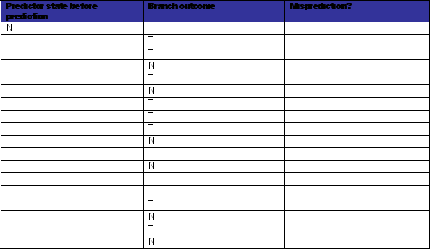
Branch Prediction. Consider the following sequence of actual outcomes for a single static branch. T means the branch is taken. N means the branch is not taken. For this question, assume that this is the only branch in the program.  (a) Assume that we try to predict this sequence with a BHT using one-bit counters. The counters in the BHT are initialized to the N state. Which of the branches in this sequence would be mis-predicted?
You may use this table for your
(a) Assume that we try to predict this sequence with a BHT using one-bit counters. The counters in the BHT are initialized to the N state. Which of the branches in this sequence would be mis-predicted?You may use this table for your
Question
Question
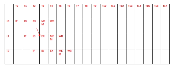
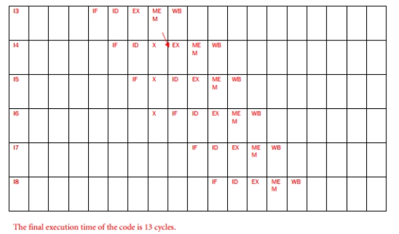
Consider the following assembly language code:
I0: ADD R4 = R1 + R0; I1: SUB R9 = R3 - R4; I2: ADD R4 = R5 + R6;
I3: LDW R2 = MEM[R3 + 100]; I4: LDW R2 = MEM[R2 + 0]; I5: STW MEM[R4 + 100] = R2; I6: AND R2 = R2 & R1;
I7: BEQ R9 == R1, Target; I8: AND R9 = R9 & R1;
Consider a pipeline with forwarding, hazard detection, and 1 delay slot for branches. The
pipeline is the typical 5-stage IF, ID, EX, MEM, WB MIPS design. For the above code, complete the pipeline diagram below (instructions on the left, cycles on top) for the code. Insert the characters IF, ID, EX, MEM, WB for each instruction in the boxes. Assume that there two levels of bypassing, that the second half of the decode stage performs a read of source registers, and that the first half of the write-back stage writes to the register file.
Label all data stalls (Draw an X in the box). Label all data forwards that the forwarding unit detects (arrow between the stages handing off the data and the stages receiving the data). What is the final execution time of the code?![Consider the following assembly language code: I0: ADD R4 = R1 + R0; I1: SUB R9 = R3 - R4; I2: ADD R4 = R5 + R6; I3: LDW R2 = MEM[R3 + 100]; I4: LDW R2 = MEM[R2 + 0]; I5: STW MEM[R4 + 100] = R2; I6: AND R2 = R2 & R1; I7: BEQ R9 == R1, Target; I8: AND R9 = R9 & R1; Consider a pipeline with forwarding, hazard detection, and 1 delay slot for branches. The pipeline is the typical 5-stage IF, ID, EX, MEM, WB MIPS design. For the above code, complete the pipeline diagram below (instructions on the left, cycles on top) for the code. Insert the characters IF, ID, EX, MEM, WB for each instruction in the boxes. Assume that there two levels of bypassing, that the second half of the decode stage performs a read of source registers, and that the first half of the write-back stage writes to the register file. Label all data stalls (Draw an X in the box). Label all data forwards that the forwarding unit detects (arrow between the stages handing off the data and the stages receiving the data). What is the final execution time of the code? <div style=padding-top: 35px>](https://d2lvgg3v3hfg70.cloudfront.net/TB5290/11eb4b6a_2491_bf79_9bf3_514ad1137c99_TB5290_00.jpg)
I0: ADD R4 = R1 + R0; I1: SUB R9 = R3 - R4; I2: ADD R4 = R5 + R6;
I3: LDW R2 = MEM[R3 + 100]; I4: LDW R2 = MEM[R2 + 0]; I5: STW MEM[R4 + 100] = R2; I6: AND R2 = R2 & R1;
I7: BEQ R9 == R1, Target; I8: AND R9 = R9 & R1;
Consider a pipeline with forwarding, hazard detection, and 1 delay slot for branches. The
pipeline is the typical 5-stage IF, ID, EX, MEM, WB MIPS design. For the above code, complete the pipeline diagram below (instructions on the left, cycles on top) for the code. Insert the characters IF, ID, EX, MEM, WB for each instruction in the boxes. Assume that there two levels of bypassing, that the second half of the decode stage performs a read of source registers, and that the first half of the write-back stage writes to the register file.
Label all data stalls (Draw an X in the box). Label all data forwards that the forwarding unit detects (arrow between the stages handing off the data and the stages receiving the data). What is the final execution time of the code?
Question
Branch Prediction. Consider the following sequence of actual outcomes for a single static branch. T means the branch is taken. N means the branch is not taken. For this question, assume that this is the only branch in the program.
(b) Now, assume a two-level branch predictor that uses one bit of branch history-i.e., a one-bit BHR. Since there is only one branch in the program, it does not matter how the BHR is concatenated with the branch PC to index the BHT. Assume that the BHT uses one-bit counters and that, again, all entries are initialized to N. Which of the branches in this sequence would be mis-predicted? Use the table below.
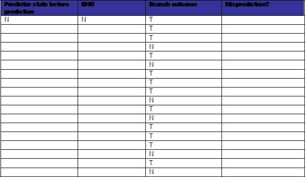
(b) Now, assume a two-level branch predictor that uses one bit of branch history-i.e., a one-bit BHR. Since there is only one branch in the program, it does not matter how the BHR is concatenated with the branch PC to index the BHT. Assume that the BHT uses one-bit counters and that, again, all entries are initialized to N. Which of the branches in this sequence would be mis-predicted? Use the table below.
Question
For the MIPS datapath shown below, several lines are marked with "X". For each one:
Describe in words the negative consequence of cutting this line relative to the working, unmodified processor.
Provide a snippet of code that will fail
Provide a snippet of code that will still work
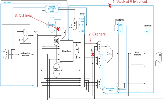
Describe in words the negative consequence of cutting this line relative to the working, unmodified processor.
Provide a snippet of code that will fail
Provide a snippet of code that will still work
Question
This problem covers your knowledge of branch prediction. The figure below illustrates three possible predictors.
Last taken predicts taken when 1
Up-Down (saturating counter) predicts taken when 11 and 10
Automata A3 predicts taken when 11 and 10
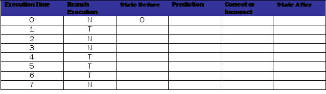
Fill out the tables below and on the next page for each branch predictor. The execution pattern for the branch is NTNNTTTN.
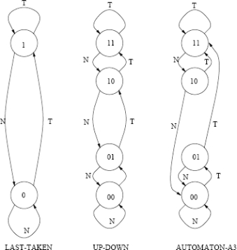 Table 1: Table for last-taken branch predictor
Last taken predicts taken when 1
Up-Down (saturating counter) predicts taken when 11 and 10
Automata A3 predicts taken when 11 and 10
Fill out the tables below and on the next page for each branch predictor. The execution pattern for the branch is NTNNTTTN.
Table 1: Table for last-taken branch predictor Question
The classic 5-stage pipeline seen in Section 4.5 is IF, ID, EX, MEM, WB. This pipeline is designed specifically to execute the MIPS instruction set. MIPS is a load store architecture that performs one memory operation per instruction, hence a single MEM stage in the pipeline suffices. Also, its most common addressing mode is register displacement addressing. The EX stage is placed before the MEM stage to allow it to be used for address calculation. In this question we will consider a variation in the MIPS instruction set and the interactions of this variation with the pipeline structure.
The particular variation we are considering involves swapping the MEM and EX stages, creating a pipeline that looks like this: IF, ID, MEM, EX, WB. This change has two effects on the instruction set. First, it prevents us from using register displacement addressing (there is no longer an EX in front of MEM to accomplish this). However, in return we can use instructions with one memory input operand, i.e., register-memory instructions. For instance: multf_m f0,f2,(r2) multiplies the contents of register f2 and the value at memory location pointed to by r2, putting the result in f0.
(a) Dropping the register displacement addressing mode is potentially a big loss, since it is the mode most frequently used in MIPS. Why is it so frequent? Give two popular software constructs whose implementation uses register displacement addressing (i.e., uses displacement addressing with non- zero displacements).
(b) What is the difference between a dependence and a hazard?
(c) In this question we will work with the SAXPY loop.
do I = 0,N
Z[I] = A*X[I] + Y[I]
Here is the new assembly code.
0: slli r2,r1,#3 // I is in r1 1: addi r3,r2,#X
2: multf_m f2,f0,(r3) // A is in f0 3: addi r4,r2,#Y
4: addf_m f4,f2,(r4)
5: addi r4,r2,#Z
6: sf f4,(r4)
7: addi r1,r1,#1
8: slei r6,r1,r5 // N is in r5 9: bnez r6,#0
Using the instruction numbers, label the data and control dependences.
(d) Fill in the pipeline diagram for code for the new SAXPY loop. Label the stalls as d* for data-hazard stalls and s* for structural stalls. What is the latency of a single iteration? (The number of cycles between the completion of two successive #0 instructions). For this question, assume that FP addition takes 2 cycles, FP multiplication takes 3 cycles and that all other operations take a single cycle. The functional units are not pipelined. The FP adder, FP multiplier and integer ALU are all separate functional units, such that there are no structural hazards between them. The register file is written by the WB stage in the first half of a clock cycle and is read by the ID stage in the second half of a clock cycle. In addition, the processor has full forwarding. The processor stalls on branches until the outcome is available which is at the end of the EX stage. The processor has no provisions for maintaining "precise state".![The classic 5-stage pipeline seen in Section 4.5 is IF, ID, EX, MEM, WB. This pipeline is designed specifically to execute the MIPS instruction set. MIPS is a load store architecture that performs one memory operation per instruction, hence a single MEM stage in the pipeline suffices. Also, its most common addressing mode is register displacement addressing. The EX stage is placed before the MEM stage to allow it to be used for address calculation. In this question we will consider a variation in the MIPS instruction set and the interactions of this variation with the pipeline structure. The particular variation we are considering involves swapping the MEM and EX stages, creating a pipeline that looks like this: IF, ID, MEM, EX, WB. This change has two effects on the instruction set. First, it prevents us from using register displacement addressing (there is no longer an EX in front of MEM to accomplish this). However, in return we can use instructions with one memory input operand, i.e., register-memory instructions. For instance: multf_m f0,f2,(r2) multiplies the contents of register f2 and the value at memory location pointed to by r2, putting the result in f0. (a) Dropping the register displacement addressing mode is potentially a big loss, since it is the mode most frequently used in MIPS. Why is it so frequent? Give two popular software constructs whose implementation uses register displacement addressing (i.e., uses displacement addressing with non- zero displacements). (b) What is the difference between a dependence and a hazard? (c) In this question we will work with the SAXPY loop. do I = 0,N Z[I] = A*X[I] + Y[I] Here is the new assembly code. 0: slli r2,r1,#3 // I is in r1 1: addi r3,r2,#X 2: multf_m f2,f0,(r3) // A is in f0 3: addi r4,r2,#Y 4: addf_m f4,f2,(r4) 5: addi r4,r2,#Z 6: sf f4,(r4) 7: addi r1,r1,#1 8: slei r6,r1,r5 // N is in r5 9: bnez r6,#0 Using the instruction numbers, label the data and control dependences. (d) Fill in the pipeline diagram for code for the new SAXPY loop. Label the stalls as d* for data-hazard stalls and s* for structural stalls. What is the latency of a single iteration? (The number of cycles between the completion of two successive #0 instructions). For this question, assume that FP addition takes 2 cycles, FP multiplication takes 3 cycles and that all other operations take a single cycle. The functional units are not pipelined. The FP adder, FP multiplier and integer ALU are all separate functional units, such that there are no structural hazards between them. The register file is written by the WB stage in the first half of a clock cycle and is read by the ID stage in the second half of a clock cycle. In addition, the processor has full forwarding. The processor stalls on branches until the outcome is available which is at the end of the EX stage. The processor has no provisions for maintaining precise state. (e) In the pipeline for MIPS mentioned in the text, what is the reason for forcing non-memory operations to go through the MEM stage rather than proceeding directly to the WB stage? (f) Aside from the direct loss of register displacement addressing and the subsequent instructions required to explicitly compute addresses, what are two other disadvantages of this sort of pipeline? (g) Reduce the stalls by pipeline scheduling a single loop iteration. Show the resulting code and fill in the pipeline diagram. You do not need to show the optimal schedule for a correct response.<div style=padding-top: 35px>](https://d2lvgg3v3hfg70.cloudfront.net/TB5290/11eb4b6a_2492_a9e2_9bf3_a739b4345d52_TB5290_00.jpg) (e) In the pipeline for MIPS mentioned in the text, what is the reason for forcing non-memory operations to go through the MEM stage rather than proceeding directly to the WB stage?
(e) In the pipeline for MIPS mentioned in the text, what is the reason for forcing non-memory operations to go through the MEM stage rather than proceeding directly to the WB stage?
(f) Aside from the direct loss of register displacement addressing and the subsequent instructions required to explicitly compute addresses, what are two other disadvantages of this sort of pipeline?
(g) Reduce the stalls by pipeline scheduling a single loop iteration. Show the resulting code and fill in the pipeline diagram. You do not need to show the optimal schedule for a correct response.
The particular variation we are considering involves swapping the MEM and EX stages, creating a pipeline that looks like this: IF, ID, MEM, EX, WB. This change has two effects on the instruction set. First, it prevents us from using register displacement addressing (there is no longer an EX in front of MEM to accomplish this). However, in return we can use instructions with one memory input operand, i.e., register-memory instructions. For instance: multf_m f0,f2,(r2) multiplies the contents of register f2 and the value at memory location pointed to by r2, putting the result in f0.
(a) Dropping the register displacement addressing mode is potentially a big loss, since it is the mode most frequently used in MIPS. Why is it so frequent? Give two popular software constructs whose implementation uses register displacement addressing (i.e., uses displacement addressing with non- zero displacements).
(b) What is the difference between a dependence and a hazard?
(c) In this question we will work with the SAXPY loop.
do I = 0,N
Z[I] = A*X[I] + Y[I]
Here is the new assembly code.
0: slli r2,r1,#3 // I is in r1 1: addi r3,r2,#X
2: multf_m f2,f0,(r3) // A is in f0 3: addi r4,r2,#Y
4: addf_m f4,f2,(r4)
5: addi r4,r2,#Z
6: sf f4,(r4)
7: addi r1,r1,#1
8: slei r6,r1,r5 // N is in r5 9: bnez r6,#0
Using the instruction numbers, label the data and control dependences.
(d) Fill in the pipeline diagram for code for the new SAXPY loop. Label the stalls as d* for data-hazard stalls and s* for structural stalls. What is the latency of a single iteration? (The number of cycles between the completion of two successive #0 instructions). For this question, assume that FP addition takes 2 cycles, FP multiplication takes 3 cycles and that all other operations take a single cycle. The functional units are not pipelined. The FP adder, FP multiplier and integer ALU are all separate functional units, such that there are no structural hazards between them. The register file is written by the WB stage in the first half of a clock cycle and is read by the ID stage in the second half of a clock cycle. In addition, the processor has full forwarding. The processor stalls on branches until the outcome is available which is at the end of the EX stage. The processor has no provisions for maintaining "precise state".
(e) In the pipeline for MIPS mentioned in the text, what is the reason for forcing non-memory operations to go through the MEM stage rather than proceeding directly to the WB stage?(f) Aside from the direct loss of register displacement addressing and the subsequent instructions required to explicitly compute addresses, what are two other disadvantages of this sort of pipeline?
(g) Reduce the stalls by pipeline scheduling a single loop iteration. Show the resulting code and fill in the pipeline diagram. You do not need to show the optimal schedule for a correct response.
Question
A two-part question.
(Part A) Dependence detection
This question covers your understanding of dependences between instructions. Using the code below, list all of the dependence types (RAW, WAR, WAW). List the dependences in the respective table (example INST-X to INST-Y) by writing in the instruction numbers involved with the dependence.
I0: A = B + C; I1: C = A - B; I2: D = A + C;
I3: A = B * C * D;
I4: C = F / D;
I5: F = A ˆ G;
I6: G = F + D;
Question
Question
Question
You are given a 4-stage pipelined processor as described below.
IF: Instruction Fetch
IDE: Instruction Decode, Register Fetch, ALU evaluation, branch instructions change PC, address calculation for memory access.
MEM: memory access for load and store instructions.
WB: Write the execution result back to the register file. The writeback occurs at the 2nd half of the cycle.
Assume the delayed branching method discussed in Section 4.3. For the following program, assume that the loop will iterate 15 times. Assume that the pipeline finishes one instruction every cycle except when a branch is taken or when an interlock takes place. An interlock prevents instructions from being executed in the wrong sequence to preserve original data dependencies. Assume register bypass from both the IDE output and the MEM output. Also assume that r2 will not be needed after the execution returns.
 (a) Is there any interlock cycle in the program? If so, perform code reordering on the program and show the new program without interlock cycle.
(b) Derive the total number of cycles required to execute all instructions before and after you eliminated the interlock cycle.
(c) Fill the delay slots. Describe the code reordering and/or duplication performed. Show the same program after delay slot filling. Recall that RETURN is also a branch instruction. Use a ' to mark the new copy of a duplicated instruction. For example, if you duplicated D, name the new copy D'.
(d)Derive the total number of cycles required to execute all instructions after you filled the delay slots.
IF: Instruction Fetch
IDE: Instruction Decode, Register Fetch, ALU evaluation, branch instructions change PC, address calculation for memory access.
MEM: memory access for load and store instructions.
WB: Write the execution result back to the register file. The writeback occurs at the 2nd half of the cycle.
Assume the delayed branching method discussed in Section 4.3. For the following program, assume that the loop will iterate 15 times. Assume that the pipeline finishes one instruction every cycle except when a branch is taken or when an interlock takes place. An interlock prevents instructions from being executed in the wrong sequence to preserve original data dependencies. Assume register bypass from both the IDE output and the MEM output. Also assume that r2 will not be needed after the execution returns.
(a) Is there any interlock cycle in the program? If so, perform code reordering on the program and show the new program without interlock cycle.(b) Derive the total number of cycles required to execute all instructions before and after you eliminated the interlock cycle.
(c) Fill the delay slots. Describe the code reordering and/or duplication performed. Show the same program after delay slot filling. Recall that RETURN is also a branch instruction. Use a ' to mark the new copy of a duplicated instruction. For example, if you duplicated D, name the new copy D'.
(d)Derive the total number of cycles required to execute all instructions after you filled the delay slots.
Question
Consider the datapath below. This machine does not support code with branch delay slots. (It predicts not-taken with a 1-cycle penalty on taken branches.) For each control signal listed in the table below, determine its value at cycles 3 through 9, inclusive. Also, show the instruction occupying each stage of the pipeline in all cycles. (Assume the IF/ID write-enable line is set to the inverse of the Stall signal.)
The initial state of the machine is:
PC = 0
All pipeline registers contain 0s
All registers in the register file contain 0s. The data memory contains 0s in all locations The instruction memory contains:
00: addiu $3, $zero, 4 04: lw $4, 100($3)
08: addu $2, $4, $3
0C: beq $4, $zero, 0x14 10: addiu $3, $3, 1
14: addu $2, $2, $3
all other locations contain 0
Use data forwarding whenever possible. All mux inputs are numbered vertically from "top" to "bottom" starting at 0 as you look at the datapath in the proper landscape orientation. Also, the values for ALUOp are:
 Instruction formats:

The initial state of the machine is:
PC = 0
All pipeline registers contain 0s
All registers in the register file contain 0s. The data memory contains 0s in all locations The instruction memory contains:
00: addiu $3, $zero, 4 04: lw $4, 100($3)
08: addu $2, $4, $3
0C: beq $4, $zero, 0x14 10: addiu $3, $3, 1
14: addu $2, $2, $3
all other locations contain 0
Use data forwarding whenever possible. All mux inputs are numbered vertically from "top" to "bottom" starting at 0 as you look at the datapath in the proper landscape orientation. Also, the values for ALUOp are:
Instruction formats: Question
Question
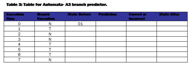
This problem covers your knowledge of branch prediction. The figure below illustrates three possible predictors.
Last taken predicts taken when 1
Up-Down (saturating counter) predicts taken when 11 and 10
Automata A3 predicts taken when 11 and 10
Fill out the tables below and on the next page for each branch predictor. The execution pattern for the branch is NTNNTTTN.
 Table 2: Table for saturating counter (up-down) branch predictor.
 Calculate the prediction rates of the three branch predictors:
Last taken predicts taken when 1
Up-Down (saturating counter) predicts taken when 11 and 10
Automata A3 predicts taken when 11 and 10
Fill out the tables below and on the next page for each branch predictor. The execution pattern for the branch is NTNNTTTN.
Table 2: Table for saturating counter (up-down) branch predictor. Calculate the prediction rates of the three branch predictors: Question
This is a three-part question about critical path calculation. Consider a simple single- cycle implementation of MIPS ISA. The operation times for the major functional components for this machine are as follows:
![This is a three-part question about critical path calculation. Consider a simple single- cycle implementation of MIPS ISA. The operation times for the major functional components for this machine are as follows: Below is a copy of the MIPS single-cycle datapath design. In this implementation the clock cycle is determined by the longest possible path in the machine. The critical paths for the different instruction types that need to be considered are: R-format, Load-word, and store-word. All instructions have the same instruction fetch and decode steps. The basic register transfer of the instructions are: Fetch/Decode: Instruction <- IMEM[PC]; R-type: R[rd] <- R[rs] op R[rt]; PC <- PC + 4; load: R[rt] <- DMEM[ R[rs] + signext(offset)]; PC <- PC +4; store: DMEM[ R[rs] + signext(offset)] <- R[Rt]; PC <- PC +4; (Part A) In the table below, indicate the components that determine the critical path for the respective instruction, in the order that the critical path occurs. If a component is used, but not part of the critical path of the instruction (ie happens in parallel with another component), it should not be in the table. The register file is used for reading and for writing; it will appear twice for some instructions. All instruction begin by reading the PC register with a latency of 2ns. <div style=padding-top: 35px>](https://d2lvgg3v3hfg70.cloudfront.net/TB5290/11eb4b6a_2494_0978_9bf3_dbe33be16b90_TB5290_00.jpg) Below is a copy of the MIPS single-cycle datapath design. In this implementation the clock cycle is determined by the longest possible path in the machine. The critical paths for the different instruction types that need to be considered are: R-format, Load-word, and store-word. All instructions have the same instruction fetch and decode steps. The basic register transfer of the instructions are:
Below is a copy of the MIPS single-cycle datapath design. In this implementation the clock cycle is determined by the longest possible path in the machine. The critical paths for the different instruction types that need to be considered are: R-format, Load-word, and store-word. All instructions have the same instruction fetch and decode steps. The basic register transfer of the instructions are:
Fetch/Decode: Instruction <- IMEM[PC];
R-type: R[rd] <- R[rs] op R[rt]; PC <- PC + 4;
load: R[rt] <- DMEM[ R[rs] + signext(offset)]; PC <- PC +4; store: DMEM[ R[rs] + signext(offset)] <- R[Rt]; PC <- PC +4;
![This is a three-part question about critical path calculation. Consider a simple single- cycle implementation of MIPS ISA. The operation times for the major functional components for this machine are as follows: Below is a copy of the MIPS single-cycle datapath design. In this implementation the clock cycle is determined by the longest possible path in the machine. The critical paths for the different instruction types that need to be considered are: R-format, Load-word, and store-word. All instructions have the same instruction fetch and decode steps. The basic register transfer of the instructions are: Fetch/Decode: Instruction <- IMEM[PC]; R-type: R[rd] <- R[rs] op R[rt]; PC <- PC + 4; load: R[rt] <- DMEM[ R[rs] + signext(offset)]; PC <- PC +4; store: DMEM[ R[rs] + signext(offset)] <- R[Rt]; PC <- PC +4; (Part A) In the table below, indicate the components that determine the critical path for the respective instruction, in the order that the critical path occurs. If a component is used, but not part of the critical path of the instruction (ie happens in parallel with another component), it should not be in the table. The register file is used for reading and for writing; it will appear twice for some instructions. All instruction begin by reading the PC register with a latency of 2ns. <div style=padding-top: 35px>](https://d2lvgg3v3hfg70.cloudfront.net/TB5290/11eb4b6a_2494_0979_9bf3_ff0434f0e554_TB5290_00.jpg) (Part A)
(Part A)
In the table below, indicate the components that determine the critical path for the respective instruction, in the order that the critical path occurs. If a component is used, but not part of the critical path of the instruction (ie happens in parallel with another component), it should not be in the table. The register file is used for reading and for writing; it will appear twice for some instructions. All instruction begin by reading the PC register with a latency of 2ns.
![This is a three-part question about critical path calculation. Consider a simple single- cycle implementation of MIPS ISA. The operation times for the major functional components for this machine are as follows: Below is a copy of the MIPS single-cycle datapath design. In this implementation the clock cycle is determined by the longest possible path in the machine. The critical paths for the different instruction types that need to be considered are: R-format, Load-word, and store-word. All instructions have the same instruction fetch and decode steps. The basic register transfer of the instructions are: Fetch/Decode: Instruction <- IMEM[PC]; R-type: R[rd] <- R[rs] op R[rt]; PC <- PC + 4; load: R[rt] <- DMEM[ R[rs] + signext(offset)]; PC <- PC +4; store: DMEM[ R[rs] + signext(offset)] <- R[Rt]; PC <- PC +4; (Part A) In the table below, indicate the components that determine the critical path for the respective instruction, in the order that the critical path occurs. If a component is used, but not part of the critical path of the instruction (ie happens in parallel with another component), it should not be in the table. The register file is used for reading and for writing; it will appear twice for some instructions. All instruction begin by reading the PC register with a latency of 2ns. <div style=padding-top: 35px>](https://d2lvgg3v3hfg70.cloudfront.net/TB5290/11eb4b6a_2494_097a_9bf3_cd586c59e320_TB5290_00.jpg)
Below is a copy of the MIPS single-cycle datapath design. In this implementation the clock cycle is determined by the longest possible path in the machine. The critical paths for the different instruction types that need to be considered are: R-format, Load-word, and store-word. All instructions have the same instruction fetch and decode steps. The basic register transfer of the instructions are:Fetch/Decode: Instruction <- IMEM[PC];
R-type: R[rd] <- R[rs] op R[rt]; PC <- PC + 4;
load: R[rt] <- DMEM[ R[rs] + signext(offset)]; PC <- PC +4; store: DMEM[ R[rs] + signext(offset)] <- R[Rt]; PC <- PC +4;
(Part A)In the table below, indicate the components that determine the critical path for the respective instruction, in the order that the critical path occurs. If a component is used, but not part of the critical path of the instruction (ie happens in parallel with another component), it should not be in the table. The register file is used for reading and for writing; it will appear twice for some instructions. All instruction begin by reading the PC register with a latency of 2ns.
Question
Consider the following data path diagram:
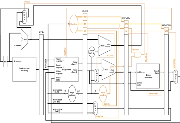 (a) Discuss the functionality of the RegDst and the ALUSrc control wires.
(b) Next, modify the diagram to indicate the datapath changes (and any additional multiplexing) needed to provide bypassing from EX to EX for all possible RAW hazards on arithmetic instructions. How does ALUSrc change when bypassing is added?
(a) Discuss the functionality of the RegDst and the ALUSrc control wires.(b) Next, modify the diagram to indicate the datapath changes (and any additional multiplexing) needed to provide bypassing from EX to EX for all possible RAW hazards on arithmetic instructions. How does ALUSrc change when bypassing is added?
Question
Question
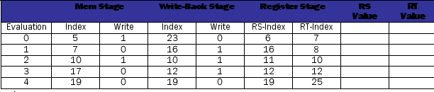
Forwarding logic design. For this problem you are to design a forwarding unit for a 5- stage pipeline processor. The forwarding unit returns the value to be forwarded to the current instruction. There are three places that the values for register RS and register RT can come from: decode stage (register file), memory stage, and write-back stage. 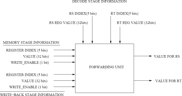 The write-back and memory stage information consists of: _INDEX- explaining which inflight register index is to be written _VALUE- the value that is to be written _ENABLE- whether or not the instruction in the stage is writing.
The decode stage simply states the register index (for RS and RT) and the corresponding register value from the register file.
Generally three values could exist, one of which the forwarding unit should choose for each of the RS and RT register value requests. The memory stage has value MEM, the write-back stage has value WB, and the register file has value RS-REG or RT-REG.
Using the table below which contains information about all of the instruction stages, indicate which value should be forwarded to the current instruction: MEM, WB, RS-REG, or RT-REG. Each line represents a Forwarding unit evaluation; there is no connection between evaluation lines in the table. You do not need to worry about hazard detection, only value bypassing.
The write-back and memory stage information consists of: _INDEX- explaining which inflight register index is to be written _VALUE- the value that is to be written _ENABLE- whether or not the instruction in the stage is writing.The decode stage simply states the register index (for RS and RT) and the corresponding register value from the register file.
Generally three values could exist, one of which the forwarding unit should choose for each of the RS and RT register value requests. The memory stage has value MEM, the write-back stage has value WB, and the register file has value RS-REG or RT-REG.
Using the table below which contains information about all of the instruction stages, indicate which value should be forwarded to the current instruction: MEM, WB, RS-REG, or RT-REG. Each line represents a Forwarding unit evaluation; there is no connection between evaluation lines in the table. You do not need to worry about hazard detection, only value bypassing.
Question
This is a three-part question about critical path calculation. Consider a simple single- cycle implementation of MIPS ISA. The operation times for the major functional components for this machine are as follows:
![This is a three-part question about critical path calculation. Consider a simple single- cycle implementation of MIPS ISA. The operation times for the major functional components for this machine are as follows: Below is a copy of the MIPS single-cycle datapath design. In this implementation the clock cycle is determined by the longest possible path in the machine. The critical paths for the different instruction types that need to be considered are: R-format, Load-word, and store-word. All instructions have the same instruction fetch and decode steps. The basic register transfer of the instructions are: Fetch/Decode: Instruction <- IMEM[PC]; R-type: R[rd] <- R[rs] op R[rt]; PC <- PC + 4; Load: R[rt] <- DMEM[ R[rs] + signext(offset)]; PC <- PC +4; store: DMEM[ R[rs] + signext(offset)] <- R[Rt]; PC <- PC +4; (Part B) Place the latencies of the components that you have decided for the critical path of each instruction in the table below. Compute the sum of each of the component latencies for each instruction. <div style=padding-top: 35px>](https://d2lvgg3v3hfg70.cloudfront.net/TB5290/11eb4b6a_2494_308c_9bf3_1111947a1a32_TB5290_00.jpg) Below is a copy of the MIPS single-cycle datapath design. In this implementation the clock cycle is determined by the longest possible path in the machine. The critical paths for the different instruction types that need to be considered are: R-format, Load-word, and store-word. All instructions have the same instruction fetch and decode steps. The basic register transfer of the instructions are:
Below is a copy of the MIPS single-cycle datapath design. In this implementation the clock cycle is determined by the longest possible path in the machine. The critical paths for the different instruction types that need to be considered are: R-format, Load-word, and store-word. All instructions have the same instruction fetch and decode steps. The basic register transfer of the instructions are:
Fetch/Decode: Instruction <- IMEM[PC];
R-type: R[rd] <- R[rs] op R[rt]; PC <- PC + 4;
Load: R[rt] <- DMEM[ R[rs] + signext(offset)]; PC <- PC +4; store: DMEM[ R[rs] + signext(offset)] <- R[Rt]; PC <- PC +4;
![This is a three-part question about critical path calculation. Consider a simple single- cycle implementation of MIPS ISA. The operation times for the major functional components for this machine are as follows: Below is a copy of the MIPS single-cycle datapath design. In this implementation the clock cycle is determined by the longest possible path in the machine. The critical paths for the different instruction types that need to be considered are: R-format, Load-word, and store-word. All instructions have the same instruction fetch and decode steps. The basic register transfer of the instructions are: Fetch/Decode: Instruction <- IMEM[PC]; R-type: R[rd] <- R[rs] op R[rt]; PC <- PC + 4; Load: R[rt] <- DMEM[ R[rs] + signext(offset)]; PC <- PC +4; store: DMEM[ R[rs] + signext(offset)] <- R[Rt]; PC <- PC +4; (Part B) Place the latencies of the components that you have decided for the critical path of each instruction in the table below. Compute the sum of each of the component latencies for each instruction. <div style=padding-top: 35px>](https://d2lvgg3v3hfg70.cloudfront.net/TB5290/11eb4b6a_2494_308d_9bf3_8df5a1477a4c_TB5290_00.jpg) (Part B)
(Part B)
Place the latencies of the components that you have decided for the critical path of each instruction in the table below. Compute the sum of each of the component latencies for each instruction.
![This is a three-part question about critical path calculation. Consider a simple single- cycle implementation of MIPS ISA. The operation times for the major functional components for this machine are as follows: Below is a copy of the MIPS single-cycle datapath design. In this implementation the clock cycle is determined by the longest possible path in the machine. The critical paths for the different instruction types that need to be considered are: R-format, Load-word, and store-word. All instructions have the same instruction fetch and decode steps. The basic register transfer of the instructions are: Fetch/Decode: Instruction <- IMEM[PC]; R-type: R[rd] <- R[rs] op R[rt]; PC <- PC + 4; Load: R[rt] <- DMEM[ R[rs] + signext(offset)]; PC <- PC +4; store: DMEM[ R[rs] + signext(offset)] <- R[Rt]; PC <- PC +4; (Part B) Place the latencies of the components that you have decided for the critical path of each instruction in the table below. Compute the sum of each of the component latencies for each instruction. <div style=padding-top: 35px>](https://d2lvgg3v3hfg70.cloudfront.net/TB5290/11eb4b6a_2494_579e_9bf3_c3973b070924_TB5290_00.jpg)
Below is a copy of the MIPS single-cycle datapath design. In this implementation the clock cycle is determined by the longest possible path in the machine. The critical paths for the different instruction types that need to be considered are: R-format, Load-word, and store-word. All instructions have the same instruction fetch and decode steps. The basic register transfer of the instructions are:Fetch/Decode: Instruction <- IMEM[PC];
R-type: R[rd] <- R[rs] op R[rt]; PC <- PC + 4;
Load: R[rt] <- DMEM[ R[rs] + signext(offset)]; PC <- PC +4; store: DMEM[ R[rs] + signext(offset)] <- R[Rt]; PC <- PC +4;
(Part B)Place the latencies of the components that you have decided for the critical path of each instruction in the table below. Compute the sum of each of the component latencies for each instruction.
Question
This is a three-part question about critical path calculation. Consider a simple single- cycle implementation of MIPS ISA. The operation times for the major functional components for this machine are as follows:
-![This is a three-part question about critical path calculation. Consider a simple single- cycle implementation of MIPS ISA. The operation times for the major functional components for this machine are as follows: - Below is a copy of the MIPS single-cycle datapath design. In this implementation the clock cycle is determined by the longest possible path in the machine. The critical paths for the different instruction types that need to be considered are: R-format, Load-word, and store-word. All instructions have the same instruction fetch and decode steps. The basic register transfer of the instructions are: Fetch/Decode: Instruction <- IMEM[PC]; R-type: R[rd] <- R[rs] op R[rt]; PC <- PC + 4; load: R[rt] <- DMEM[ R[rs] + signext(offset)]; PC <- PC +4; store: DMEM[ R[rs] + signext(offset)] <- R[Rt]; PC <- PC +4; (Part C) Use the total latency column to derive the following critical path information: \bullet Given the data path latencies above, which instruction determines the overall machine critical path (latency)? \bullet What will be the resultant clock cycle time of the machine based on the critical path instruction? \bullet What frequency will the machine run?<div style=padding-top: 35px>](https://d2lvgg3v3hfg70.cloudfront.net/TB5290/11eb4b6a_2494_7eb0_9bf3_41ea677c4ee2_TB5290_00.jpg) Below is a copy of the MIPS single-cycle datapath design. In this implementation the clock cycle is determined by the longest possible path in the machine. The critical paths for the different instruction types that need to be considered are: R-format, Load-word, and store-word. All instructions have the same instruction fetch and decode steps. The basic register transfer of the instructions are:
Below is a copy of the MIPS single-cycle datapath design. In this implementation the clock cycle is determined by the longest possible path in the machine. The critical paths for the different instruction types that need to be considered are: R-format, Load-word, and store-word. All instructions have the same instruction fetch and decode steps. The basic register transfer of the instructions are:
Fetch/Decode: Instruction <- IMEM[PC];
R-type: R[rd] <- R[rs] op R[rt]; PC <- PC + 4;
load: R[rt] <- DMEM[ R[rs] + signext(offset)]; PC <- PC +4; store: DMEM[ R[rs] + signext(offset)] <- R[Rt]; PC <- PC +4;
![This is a three-part question about critical path calculation. Consider a simple single- cycle implementation of MIPS ISA. The operation times for the major functional components for this machine are as follows: - Below is a copy of the MIPS single-cycle datapath design. In this implementation the clock cycle is determined by the longest possible path in the machine. The critical paths for the different instruction types that need to be considered are: R-format, Load-word, and store-word. All instructions have the same instruction fetch and decode steps. The basic register transfer of the instructions are: Fetch/Decode: Instruction <- IMEM[PC]; R-type: R[rd] <- R[rs] op R[rt]; PC <- PC + 4; load: R[rt] <- DMEM[ R[rs] + signext(offset)]; PC <- PC +4; store: DMEM[ R[rs] + signext(offset)] <- R[Rt]; PC <- PC +4; (Part C) Use the total latency column to derive the following critical path information: \bullet Given the data path latencies above, which instruction determines the overall machine critical path (latency)? \bullet What will be the resultant clock cycle time of the machine based on the critical path instruction? \bullet What frequency will the machine run?<div style=padding-top: 35px>](https://d2lvgg3v3hfg70.cloudfront.net/TB5290/11eb4b6a_2494_7eb1_9bf3_0716deaf7ac4_TB5290_00.jpg) (Part C)
(Part C)
Use the total latency column to derive the following critical path information:
Given the data path latencies above, which instruction determines the overall machine critical path (latency)?
What will be the resultant clock cycle time of the machine based on the critical path instruction?
What frequency will the machine run?
-
Below is a copy of the MIPS single-cycle datapath design. In this implementation the clock cycle is determined by the longest possible path in the machine. The critical paths for the different instruction types that need to be considered are: R-format, Load-word, and store-word. All instructions have the same instruction fetch and decode steps. The basic register transfer of the instructions are:Fetch/Decode: Instruction <- IMEM[PC];
R-type: R[rd] <- R[rs] op R[rt]; PC <- PC + 4;
load: R[rt] <- DMEM[ R[rs] + signext(offset)]; PC <- PC +4; store: DMEM[ R[rs] + signext(offset)] <- R[Rt]; PC <- PC +4;
(Part C)Use the total latency column to derive the following critical path information:
Given the data path latencies above, which instruction determines the overall machine critical path (latency)?
What will be the resultant clock cycle time of the machine based on the critical path instruction?
What frequency will the machine run?
Question
Question

Unlock Deck
Sign up to unlock the cards in this deck!
Unlock Deck
Unlock Deck
1/22
Play
Full screen (f)
Deck 4: The Processor
1
Branch Prediction. Consider the following sequence of actual outcomes for a single static branch. T means the branch is taken. N means the branch is not taken. For this question, assume that this is the only branch in the program. (a) Assume that we try to predict this sequence with a BHT using one-bit counters. The counters in the BHT are initialized to the N state. Which of the branches in this sequence would be mis-predicted?
You may use this table for your
(a) Assume that we try to predict this sequence with a BHT using one-bit counters. The counters in the BHT are initialized to the N state. Which of the branches in this sequence would be mis-predicted?You may use this table for your
2
Using any ILP optimization, double the performance of the following loop, or explain why it is not possible. The machine can only do one branch per cycle, but has infinite resources otherwise.
r1 = ... ; r1 is head pointer to a linked list r3 = 0
LOOP:
r2 = M[r1 + 8]
r3 = r3 + r2 r1 = M[r1]
branch r1 != 0, LOOP
... = r3 ; r3 is used when loop complete
r1 = ... ; r1 is head pointer to a linked list r3 = 0
LOOP:
r2 = M[r1 + 8]
r3 = r3 + r2 r1 = M[r1]
branch r1 != 0, LOOP
... = r3 ; r3 is used when loop complete
By performing the following code reordering we can avoid a 1-cycle stall due to a dependence between the first and second instructions of the loop:
r1 = ... ; r1 is head pointer to a linked list r3 = 0
LOOP:
r3 = r3 + r2 r2 = M[r1 + 8] r1 = M[r1]
branch r1 != 0, LOOP
... = r3 ; r3 is used when loop complete
r1 = ... ; r1 is head pointer to a linked list r3 = 0
LOOP:
r3 = r3 + r2 r2 = M[r1 + 8] r1 = M[r1]
branch r1 != 0, LOOP
... = r3 ; r3 is used when loop complete
3
Consider the following assembly language code:
I0: ADD R4 = R1 + R0; I1: SUB R9 = R3 - R4; I2: ADD R4 = R5 + R6;
I3: LDW R2 = MEM[R3 + 100]; I4: LDW R2 = MEM[R2 + 0]; I5: STW MEM[R4 + 100] = R2; I6: AND R2 = R2 & R1;
I7: BEQ R9 == R1, Target; I8: AND R9 = R9 & R1;
Consider a pipeline with forwarding, hazard detection, and 1 delay slot for branches. The
pipeline is the typical 5-stage IF, ID, EX, MEM, WB MIPS design. For the above code, complete the pipeline diagram below (instructions on the left, cycles on top) for the code. Insert the characters IF, ID, EX, MEM, WB for each instruction in the boxes. Assume that there two levels of bypassing, that the second half of the decode stage performs a read of source registers, and that the first half of the write-back stage writes to the register file.
Label all data stalls (Draw an X in the box). Label all data forwards that the forwarding unit detects (arrow between the stages handing off the data and the stages receiving the data). What is the final execution time of the code?

4
Branch Prediction. Consider the following sequence of actual outcomes for a single static branch. T means the branch is taken. N means the branch is not taken. For this question, assume that this is the only branch in the program.
(b) Now, assume a two-level branch predictor that uses one bit of branch history-i.e., a one-bit BHR. Since there is only one branch in the program, it does not matter how the BHR is concatenated with the branch PC to index the BHT. Assume that the BHT uses one-bit counters and that, again, all entries are initialized to N. Which of the branches in this sequence would be mis-predicted? Use the table below.
(b) Now, assume a two-level branch predictor that uses one bit of branch history-i.e., a one-bit BHR. Since there is only one branch in the program, it does not matter how the BHR is concatenated with the branch PC to index the BHT. Assume that the BHT uses one-bit counters and that, again, all entries are initialized to N. Which of the branches in this sequence would be mis-predicted? Use the table below.
Unlock Deck
Unlock for access to all 22 flashcards in this deck.
Unlock Deck
k this deck
5
For the MIPS datapath shown below, several lines are marked with "X". For each one:
Describe in words the negative consequence of cutting this line relative to the working, unmodified processor.
Provide a snippet of code that will fail
Provide a snippet of code that will still work
Describe in words the negative consequence of cutting this line relative to the working, unmodified processor.
Provide a snippet of code that will fail
Provide a snippet of code that will still work
Unlock Deck
Unlock for access to all 22 flashcards in this deck.
Unlock Deck
k this deck
6
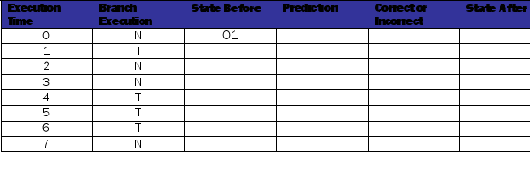
This problem covers your knowledge of branch prediction. The figure below illustrates three possible predictors.
Last taken predicts taken when 1
Up-Down (saturating counter) predicts taken when 11 and 10
Automata A3 predicts taken when 11 and 10
Fill out the tables below and on the next page for each branch predictor. The execution pattern for the branch is NTNNTTTN.
Table 1: Table for last-taken branch predictor
Last taken predicts taken when 1
Up-Down (saturating counter) predicts taken when 11 and 10
Automata A3 predicts taken when 11 and 10
Fill out the tables below and on the next page for each branch predictor. The execution pattern for the branch is NTNNTTTN.
Table 1: Table for last-taken branch predictor Unlock Deck
Unlock for access to all 22 flashcards in this deck.
Unlock Deck
k this deck
7
The classic 5-stage pipeline seen in Section 4.5 is IF, ID, EX, MEM, WB. This pipeline is designed specifically to execute the MIPS instruction set. MIPS is a load store architecture that performs one memory operation per instruction, hence a single MEM stage in the pipeline suffices. Also, its most common addressing mode is register displacement addressing. The EX stage is placed before the MEM stage to allow it to be used for address calculation. In this question we will consider a variation in the MIPS instruction set and the interactions of this variation with the pipeline structure.
The particular variation we are considering involves swapping the MEM and EX stages, creating a pipeline that looks like this: IF, ID, MEM, EX, WB. This change has two effects on the instruction set. First, it prevents us from using register displacement addressing (there is no longer an EX in front of MEM to accomplish this). However, in return we can use instructions with one memory input operand, i.e., register-memory instructions. For instance: multf_m f0,f2,(r2) multiplies the contents of register f2 and the value at memory location pointed to by r2, putting the result in f0.
(a) Dropping the register displacement addressing mode is potentially a big loss, since it is the mode most frequently used in MIPS. Why is it so frequent? Give two popular software constructs whose implementation uses register displacement addressing (i.e., uses displacement addressing with non- zero displacements).
(b) What is the difference between a dependence and a hazard?
(c) In this question we will work with the SAXPY loop.
do I = 0,N
Z[I] = A*X[I] + Y[I]
Here is the new assembly code.
0: slli r2,r1,#3 // I is in r1 1: addi r3,r2,#X
2: multf_m f2,f0,(r3) // A is in f0 3: addi r4,r2,#Y
4: addf_m f4,f2,(r4)
5: addi r4,r2,#Z
6: sf f4,(r4)
7: addi r1,r1,#1
8: slei r6,r1,r5 // N is in r5 9: bnez r6,#0
Using the instruction numbers, label the data and control dependences.
(d) Fill in the pipeline diagram for code for the new SAXPY loop. Label the stalls as d* for data-hazard stalls and s* for structural stalls. What is the latency of a single iteration? (The number of cycles between the completion of two successive #0 instructions). For this question, assume that FP addition takes 2 cycles, FP multiplication takes 3 cycles and that all other operations take a single cycle. The functional units are not pipelined. The FP adder, FP multiplier and integer ALU are all separate functional units, such that there are no structural hazards between them. The register file is written by the WB stage in the first half of a clock cycle and is read by the ID stage in the second half of a clock cycle. In addition, the processor has full forwarding. The processor stalls on branches until the outcome is available which is at the end of the EX stage. The processor has no provisions for maintaining "precise state". (e) In the pipeline for MIPS mentioned in the text, what is the reason for forcing non-memory operations to go through the MEM stage rather than proceeding directly to the WB stage?
(f) Aside from the direct loss of register displacement addressing and the subsequent instructions required to explicitly compute addresses, what are two other disadvantages of this sort of pipeline?
(g) Reduce the stalls by pipeline scheduling a single loop iteration. Show the resulting code and fill in the pipeline diagram. You do not need to show the optimal schedule for a correct response.
The particular variation we are considering involves swapping the MEM and EX stages, creating a pipeline that looks like this: IF, ID, MEM, EX, WB. This change has two effects on the instruction set. First, it prevents us from using register displacement addressing (there is no longer an EX in front of MEM to accomplish this). However, in return we can use instructions with one memory input operand, i.e., register-memory instructions. For instance: multf_m f0,f2,(r2) multiplies the contents of register f2 and the value at memory location pointed to by r2, putting the result in f0.
(a) Dropping the register displacement addressing mode is potentially a big loss, since it is the mode most frequently used in MIPS. Why is it so frequent? Give two popular software constructs whose implementation uses register displacement addressing (i.e., uses displacement addressing with non- zero displacements).
(b) What is the difference between a dependence and a hazard?
(c) In this question we will work with the SAXPY loop.
do I = 0,N
Z[I] = A*X[I] + Y[I]
Here is the new assembly code.
0: slli r2,r1,#3 // I is in r1 1: addi r3,r2,#X
2: multf_m f2,f0,(r3) // A is in f0 3: addi r4,r2,#Y
4: addf_m f4,f2,(r4)
5: addi r4,r2,#Z
6: sf f4,(r4)
7: addi r1,r1,#1
8: slei r6,r1,r5 // N is in r5 9: bnez r6,#0
Using the instruction numbers, label the data and control dependences.
(d) Fill in the pipeline diagram for code for the new SAXPY loop. Label the stalls as d* for data-hazard stalls and s* for structural stalls. What is the latency of a single iteration? (The number of cycles between the completion of two successive #0 instructions). For this question, assume that FP addition takes 2 cycles, FP multiplication takes 3 cycles and that all other operations take a single cycle. The functional units are not pipelined. The FP adder, FP multiplier and integer ALU are all separate functional units, such that there are no structural hazards between them. The register file is written by the WB stage in the first half of a clock cycle and is read by the ID stage in the second half of a clock cycle. In addition, the processor has full forwarding. The processor stalls on branches until the outcome is available which is at the end of the EX stage. The processor has no provisions for maintaining "precise state".
(e) In the pipeline for MIPS mentioned in the text, what is the reason for forcing non-memory operations to go through the MEM stage rather than proceeding directly to the WB stage?(f) Aside from the direct loss of register displacement addressing and the subsequent instructions required to explicitly compute addresses, what are two other disadvantages of this sort of pipeline?
(g) Reduce the stalls by pipeline scheduling a single loop iteration. Show the resulting code and fill in the pipeline diagram. You do not need to show the optimal schedule for a correct response.
Unlock Deck
Unlock for access to all 22 flashcards in this deck.
Unlock Deck
k this deck
8
A two-part question.
(Part A) Dependence detection
This question covers your understanding of dependences between instructions. Using the code below, list all of the dependence types (RAW, WAR, WAW). List the dependences in the respective table (example INST-X to INST-Y) by writing in the instruction numbers involved with the dependence.
I0: A = B + C; I1: C = A - B; I2: D = A + C;
I3: A = B * C * D;
I4: C = F / D;
I5: F = A ˆ G;
I6: G = F + D;
Unlock Deck
Unlock for access to all 22 flashcards in this deck.
Unlock Deck
k this deck
9
A two-part question.
Given four instructions, how many unique comparisons (between register sources and destinations) are necessary to find all of the RAW, WAR, and WAW dependences. Answer for the case of four instructions, and then derive a general equation for N instructions. Assume that all instructions have one register destination and two register sources.
Given four instructions, how many unique comparisons (between register sources and destinations) are necessary to find all of the RAW, WAR, and WAW dependences. Answer for the case of four instructions, and then derive a general equation for N instructions. Assume that all instructions have one register destination and two register sources.
Unlock Deck
Unlock for access to all 22 flashcards in this deck.
Unlock Deck
k this deck
10
Pipelining is used because it improves instruction throughput. Increasing the level of pipelining cuts the amount of work performed at each pipeline stage, allowing more instructions to exist in the processor at the same time and individual instructions to complete
at a more rapid rate. However, throughput will not improve as pipelining is increased indefinitely. Give two reasons for this.
at a more rapid rate. However, throughput will not improve as pipelining is increased indefinitely. Give two reasons for this.
Unlock Deck
Unlock for access to all 22 flashcards in this deck.
Unlock Deck
k this deck
11
You are given a 4-stage pipelined processor as described below.
IF: Instruction Fetch
IDE: Instruction Decode, Register Fetch, ALU evaluation, branch instructions change PC, address calculation for memory access.
MEM: memory access for load and store instructions.
WB: Write the execution result back to the register file. The writeback occurs at the 2nd half of the cycle.
Assume the delayed branching method discussed in Section 4.3. For the following program, assume that the loop will iterate 15 times. Assume that the pipeline finishes one instruction every cycle except when a branch is taken or when an interlock takes place. An interlock prevents instructions from being executed in the wrong sequence to preserve original data dependencies. Assume register bypass from both the IDE output and the MEM output. Also assume that r2 will not be needed after the execution returns.
(a) Is there any interlock cycle in the program? If so, perform code reordering on the program and show the new program without interlock cycle.
(b) Derive the total number of cycles required to execute all instructions before and after you eliminated the interlock cycle.
(c) Fill the delay slots. Describe the code reordering and/or duplication performed. Show the same program after delay slot filling. Recall that RETURN is also a branch instruction. Use a ' to mark the new copy of a duplicated instruction. For example, if you duplicated D, name the new copy D'.
(d)Derive the total number of cycles required to execute all instructions after you filled the delay slots.
IF: Instruction Fetch
IDE: Instruction Decode, Register Fetch, ALU evaluation, branch instructions change PC, address calculation for memory access.
MEM: memory access for load and store instructions.
WB: Write the execution result back to the register file. The writeback occurs at the 2nd half of the cycle.
Assume the delayed branching method discussed in Section 4.3. For the following program, assume that the loop will iterate 15 times. Assume that the pipeline finishes one instruction every cycle except when a branch is taken or when an interlock takes place. An interlock prevents instructions from being executed in the wrong sequence to preserve original data dependencies. Assume register bypass from both the IDE output and the MEM output. Also assume that r2 will not be needed after the execution returns.
(a) Is there any interlock cycle in the program? If so, perform code reordering on the program and show the new program without interlock cycle.(b) Derive the total number of cycles required to execute all instructions before and after you eliminated the interlock cycle.
(c) Fill the delay slots. Describe the code reordering and/or duplication performed. Show the same program after delay slot filling. Recall that RETURN is also a branch instruction. Use a ' to mark the new copy of a duplicated instruction. For example, if you duplicated D, name the new copy D'.
(d)Derive the total number of cycles required to execute all instructions after you filled the delay slots.
Unlock Deck
Unlock for access to all 22 flashcards in this deck.
Unlock Deck
k this deck
12
Consider the datapath below. This machine does not support code with branch delay slots. (It predicts not-taken with a 1-cycle penalty on taken branches.) For each control signal listed in the table below, determine its value at cycles 3 through 9, inclusive. Also, show the instruction occupying each stage of the pipeline in all cycles. (Assume the IF/ID write-enable line is set to the inverse of the Stall signal.)
The initial state of the machine is:
PC = 0
All pipeline registers contain 0s
All registers in the register file contain 0s. The data memory contains 0s in all locations The instruction memory contains:
00: addiu $3, $zero, 4 04: lw $4, 100($3)
08: addu $2, $4, $3
0C: beq $4, $zero, 0x14 10: addiu $3, $3, 1
14: addu $2, $2, $3
all other locations contain 0
Use data forwarding whenever possible. All mux inputs are numbered vertically from "top" to "bottom" starting at 0 as you look at the datapath in the proper landscape orientation. Also, the values for ALUOp are:
Instruction formats:
The initial state of the machine is:
PC = 0
All pipeline registers contain 0s
All registers in the register file contain 0s. The data memory contains 0s in all locations The instruction memory contains:
00: addiu $3, $zero, 4 04: lw $4, 100($3)
08: addu $2, $4, $3
0C: beq $4, $zero, 0x14 10: addiu $3, $3, 1
14: addu $2, $2, $3
all other locations contain 0
Use data forwarding whenever possible. All mux inputs are numbered vertically from "top" to "bottom" starting at 0 as you look at the datapath in the proper landscape orientation. Also, the values for ALUOp are:
Instruction formats: Unlock Deck
Unlock for access to all 22 flashcards in this deck.
Unlock Deck
k this deck
13
Structural, data and control hazards typically require a processor pipeline to stall. Listed below are a series of optimization techniques implemented in a compiler or a processor pipeline designed to reduce or eliminate stalls due to these hazards. For each of the following optimization techniques, state which pipeline hazards it addresses and how it addresses it. Some optimization techniques may address more than one hazard, so be sure to include explanations for all addressed hazards.
(a) Branch Prediction
(b) Instruction Scheduling
(c) delay slots
(d) increasing availability of functional units (ALUs, adders etc)
(e) caches
(a) Branch Prediction
(b) Instruction Scheduling
(c) delay slots
(d) increasing availability of functional units (ALUs, adders etc)
(e) caches
Unlock Deck
Unlock for access to all 22 flashcards in this deck.
Unlock Deck
k this deck
14
This problem covers your knowledge of branch prediction. The figure below illustrates three possible predictors.
Last taken predicts taken when 1
Up-Down (saturating counter) predicts taken when 11 and 10
Automata A3 predicts taken when 11 and 10
Fill out the tables below and on the next page for each branch predictor. The execution pattern for the branch is NTNNTTTN.
Table 2: Table for saturating counter (up-down) branch predictor.
Calculate the prediction rates of the three branch predictors:
Last taken predicts taken when 1
Up-Down (saturating counter) predicts taken when 11 and 10
Automata A3 predicts taken when 11 and 10
Fill out the tables below and on the next page for each branch predictor. The execution pattern for the branch is NTNNTTTN.
Table 2: Table for saturating counter (up-down) branch predictor. Calculate the prediction rates of the three branch predictors: Unlock Deck
Unlock for access to all 22 flashcards in this deck.
Unlock Deck
k this deck
14
This is a three-part question about critical path calculation. Consider a simple single- cycle implementation of MIPS ISA. The operation times for the major functional components for this machine are as follows:
Below is a copy of the MIPS single-cycle datapath design. In this implementation the clock cycle is determined by the longest possible path in the machine. The critical paths for the different instruction types that need to be considered are: R-format, Load-word, and store-word. All instructions have the same instruction fetch and decode steps. The basic register transfer of the instructions are:
Fetch/Decode: Instruction <- IMEM[PC];
R-type: R[rd] <- R[rs] op R[rt]; PC <- PC + 4;
load: R[rt] <- DMEM[ R[rs] + signext(offset)]; PC <- PC +4; store: DMEM[ R[rs] + signext(offset)] <- R[Rt]; PC <- PC +4;
(Part A)
In the table below, indicate the components that determine the critical path for the respective instruction, in the order that the critical path occurs. If a component is used, but not part of the critical path of the instruction (ie happens in parallel with another component), it should not be in the table. The register file is used for reading and for writing; it will appear twice for some instructions. All instruction begin by reading the PC register with a latency of 2ns.
Below is a copy of the MIPS single-cycle datapath design. In this implementation the clock cycle is determined by the longest possible path in the machine. The critical paths for the different instruction types that need to be considered are: R-format, Load-word, and store-word. All instructions have the same instruction fetch and decode steps. The basic register transfer of the instructions are:Fetch/Decode: Instruction <- IMEM[PC];
R-type: R[rd] <- R[rs] op R[rt]; PC <- PC + 4;
load: R[rt] <- DMEM[ R[rs] + signext(offset)]; PC <- PC +4; store: DMEM[ R[rs] + signext(offset)] <- R[Rt]; PC <- PC +4;
(Part A)In the table below, indicate the components that determine the critical path for the respective instruction, in the order that the critical path occurs. If a component is used, but not part of the critical path of the instruction (ie happens in parallel with another component), it should not be in the table. The register file is used for reading and for writing; it will appear twice for some instructions. All instruction begin by reading the PC register with a latency of 2ns.
Unlock Deck
Unlock for access to all 22 flashcards in this deck.
Unlock Deck
k this deck
15
Consider the following data path diagram:
(a) Discuss the functionality of the RegDst and the ALUSrc control wires.
(b) Next, modify the diagram to indicate the datapath changes (and any additional multiplexing) needed to provide bypassing from EX to EX for all possible RAW hazards on arithmetic instructions. How does ALUSrc change when bypassing is added?
(a) Discuss the functionality of the RegDst and the ALUSrc control wires.(b) Next, modify the diagram to indicate the datapath changes (and any additional multiplexing) needed to provide bypassing from EX to EX for all possible RAW hazards on arithmetic instructions. How does ALUSrc change when bypassing is added?
Unlock Deck
Unlock for access to all 22 flashcards in this deck.
Unlock Deck
k this deck
16
Branch Prediction. Consider the following sequence of actual outcomes for a single static branch. T means the branch is taken. N means the branch is not taken. For this question, assume that this is the only branch in the program.
(c) What is a return-address-stack? When is a return address stack updated?
(c) What is a return-address-stack? When is a return address stack updated?
Unlock Deck
Unlock for access to all 22 flashcards in this deck.
Unlock Deck
k this deck
17
Forwarding logic design. For this problem you are to design a forwarding unit for a 5- stage pipeline processor. The forwarding unit returns the value to be forwarded to the current instruction. There are three places that the values for register RS and register RT can come from: decode stage (register file), memory stage, and write-back stage. The write-back and memory stage information consists of: _INDEX- explaining which inflight register index is to be written _VALUE- the value that is to be written _ENABLE- whether or not the instruction in the stage is writing.
The decode stage simply states the register index (for RS and RT) and the corresponding register value from the register file.
Generally three values could exist, one of which the forwarding unit should choose for each of the RS and RT register value requests. The memory stage has value MEM, the write-back stage has value WB, and the register file has value RS-REG or RT-REG.
Using the table below which contains information about all of the instruction stages, indicate which value should be forwarded to the current instruction: MEM, WB, RS-REG, or RT-REG. Each line represents a Forwarding unit evaluation; there is no connection between evaluation lines in the table. You do not need to worry about hazard detection, only value bypassing.
The write-back and memory stage information consists of: _INDEX- explaining which inflight register index is to be written _VALUE- the value that is to be written _ENABLE- whether or not the instruction in the stage is writing.The decode stage simply states the register index (for RS and RT) and the corresponding register value from the register file.
Generally three values could exist, one of which the forwarding unit should choose for each of the RS and RT register value requests. The memory stage has value MEM, the write-back stage has value WB, and the register file has value RS-REG or RT-REG.
Using the table below which contains information about all of the instruction stages, indicate which value should be forwarded to the current instruction: MEM, WB, RS-REG, or RT-REG. Each line represents a Forwarding unit evaluation; there is no connection between evaluation lines in the table. You do not need to worry about hazard detection, only value bypassing.
Unlock Deck
Unlock for access to all 22 flashcards in this deck.
Unlock Deck
k this deck
18
This is a three-part question about critical path calculation. Consider a simple single- cycle implementation of MIPS ISA. The operation times for the major functional components for this machine are as follows:
Below is a copy of the MIPS single-cycle datapath design. In this implementation the clock cycle is determined by the longest possible path in the machine. The critical paths for the different instruction types that need to be considered are: R-format, Load-word, and store-word. All instructions have the same instruction fetch and decode steps. The basic register transfer of the instructions are:
Fetch/Decode: Instruction <- IMEM[PC];
R-type: R[rd] <- R[rs] op R[rt]; PC <- PC + 4;
Load: R[rt] <- DMEM[ R[rs] + signext(offset)]; PC <- PC +4; store: DMEM[ R[rs] + signext(offset)] <- R[Rt]; PC <- PC +4;
(Part B)
Place the latencies of the components that you have decided for the critical path of each instruction in the table below. Compute the sum of each of the component latencies for each instruction.
Below is a copy of the MIPS single-cycle datapath design. In this implementation the clock cycle is determined by the longest possible path in the machine. The critical paths for the different instruction types that need to be considered are: R-format, Load-word, and store-word. All instructions have the same instruction fetch and decode steps. The basic register transfer of the instructions are:Fetch/Decode: Instruction <- IMEM[PC];
R-type: R[rd] <- R[rs] op R[rt]; PC <- PC + 4;
Load: R[rt] <- DMEM[ R[rs] + signext(offset)]; PC <- PC +4; store: DMEM[ R[rs] + signext(offset)] <- R[Rt]; PC <- PC +4;
(Part B)Place the latencies of the components that you have decided for the critical path of each instruction in the table below. Compute the sum of each of the component latencies for each instruction.
Unlock Deck
Unlock for access to all 22 flashcards in this deck.
Unlock Deck
k this deck
19
This is a three-part question about critical path calculation. Consider a simple single- cycle implementation of MIPS ISA. The operation times for the major functional components for this machine are as follows:
- Below is a copy of the MIPS single-cycle datapath design. In this implementation the clock cycle is determined by the longest possible path in the machine. The critical paths for the different instruction types that need to be considered are: R-format, Load-word, and store-word. All instructions have the same instruction fetch and decode steps. The basic register transfer of the instructions are:
Fetch/Decode: Instruction <- IMEM[PC];
R-type: R[rd] <- R[rs] op R[rt]; PC <- PC + 4;
load: R[rt] <- DMEM[ R[rs] + signext(offset)]; PC <- PC +4; store: DMEM[ R[rs] + signext(offset)] <- R[Rt]; PC <- PC +4;
(Part C)
Use the total latency column to derive the following critical path information:
Given the data path latencies above, which instruction determines the overall machine critical path (latency)?
What will be the resultant clock cycle time of the machine based on the critical path instruction?
What frequency will the machine run?
-
Below is a copy of the MIPS single-cycle datapath design. In this implementation the clock cycle is determined by the longest possible path in the machine. The critical paths for the different instruction types that need to be considered are: R-format, Load-word, and store-word. All instructions have the same instruction fetch and decode steps. The basic register transfer of the instructions are:Fetch/Decode: Instruction <- IMEM[PC];
R-type: R[rd] <- R[rs] op R[rt]; PC <- PC + 4;
load: R[rt] <- DMEM[ R[rs] + signext(offset)]; PC <- PC +4; store: DMEM[ R[rs] + signext(offset)] <- R[Rt]; PC <- PC +4;
(Part C)Use the total latency column to derive the following critical path information:
Given the data path latencies above, which instruction determines the overall machine critical path (latency)?
What will be the resultant clock cycle time of the machine based on the critical path instruction?
What frequency will the machine run?
Unlock Deck
Unlock for access to all 22 flashcards in this deck.
Unlock Deck
k this deck
20
Consider a MIPS machine with a 5-stage pipeline with a cycle time of 10ns. Assume that you are executing a program where a fraction, f, of all instructions immediately follow a load upon which they are dependent.
(a) With forwarding enabled what is the total execution time for N instructions, in terms of f ?
(b) Consider a scenario where the MEM stage, along with its pipeline registers, needs 12 ns. There are now two options: add another MEM stage so that there are MEM1 and MEM2 stages or increase the cycle time to 12ns so that the MEM stage fits within the new cycle time and the number of pipeline stages remain unaffected. For a program mix with the above characteristics, when is the first option better than the second. Your answer should be based on the value of f.
(c) Embedded processors have two different memory regions - a faster scratchpad memory and a slower normal memory. Assume that in the 6 stage machine (with MEM1 and MEM2 stages), there is a region of memory that is faster and for which the correct value is obtained at the end of the MEM1 stage itself while the rest of the memory needs both MEM1 and MEM2 stages. For the sake of simplicity assume that there are two load instructions load.fast and load.slow that indicate which memory region is accessed. If 40% of the fraction f mentioned above get their value from the fast memory, how does the answer to the previous question change ?
Unlock Deck
Unlock for access to all 22 flashcards in this deck.
Unlock Deck
k this deck
21
Imagine an instruction whose function is to read four adjacent 32-bit words from memory and places them into four specified 32-bit architectural registers. Assuming the 5-stage pipeline is filled with these instructions and these instructions ONLY, what is the minimum number of register file read and write ports that would be required?
Unlock Deck
Unlock for access to all 22 flashcards in this deck.
Unlock Deck
k this deck
Unlock Deck
Unlock for access to all 22 flashcards in this deck.


