Deck 2: Solidstate Devices in Industrial Applications, Operational Amplifiers and Linear ICS
Full screen (f)
Question
Question
Question
Question
Question
Question
Question
Question
Question
Question
Question
Question
Question
Question
Question
Question
Question
Question
Question
Question
Question
Question
Question
Question
Question
Question
Question
Question
Question
Question
Question
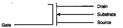
-The symbol in this graphic is a
A) P -channel enhancement mode MOSFET.
B) N -channel depletion mode MOSFET.
C) P -channel depletion mode MOSFET.
D) N -channel enhancement mode MOSFET.
Question
Question
Question
Question
Question
Question
? 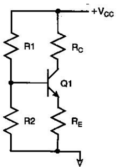
-In designing this four -resistor bias circuit, the AC gain is set by the ratio of
A) RC to RE.
B) RE to RC.
C) R1 to R2.
D) R1 to RE.
-In designing this four -resistor bias circuit, the AC gain is set by the ratio of
A) RC to RE.
B) RE to RC.
C) R1 to R2.
D) R1 to RE.
Question
Question
Question
Question
Question
Question
Question
Question
Question
Question
Question
Question
Question
Question
Question
Question
Question
Question
Question
Question
Question
Question
Question
Question
Question
Question
Question
Question
Question
Question
Question
Question
Question
Question
Question
? 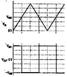
-Examine these waveforms. The most accurate description the circuit that has the VOUT for the VIN would be a __________ op amp.
A) differential
B) integrator
C) comparator
D) differentiator
E) summing
Op amp.
-Examine these waveforms. The most accurate description the circuit that has the VOUT for the VIN would be a __________ op amp.
A) differential
B) integrator
C) comparator
D) differentiator
E) summing
Op amp.
Question
Question
Question
Question
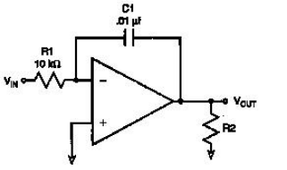
-This circuit depicts
A) a differentiator.
B) a first order high pass filter.
C) a first order low pass filter.
D) an integrator.
Question
Match the components with their function
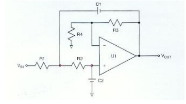
-R3 and R4
A) determines characteristics of the low pass filter
B) determines characteristics of the high pass filter
C) determines the gain
D) determines the filter type
-R3 and R4
A) determines characteristics of the low pass filter
B) determines characteristics of the high pass filter
C) determines the gain
D) determines the filter type
Question
Match the components with their function
-R1 and C1
A) determines characteristics of the low pass filter
B) determines characteristics of the high pass filter
C) determines the gain
D) determines the filter type
-R1 and C1
A) determines characteristics of the low pass filter
B) determines characteristics of the high pass filter
C) determines the gain
D) determines the filter type
Question
Match the components with their function
-R2 and C2
A) determines characteristics of the low pass filter
B) determines characteristics of the high pass filter
C) determines the gain
D) determines the filter type
-R2 and C2
A) determines characteristics of the low pass filter
B) determines characteristics of the high pass filter
C) determines the gain
D) determines the filter type

Unlock Deck
Sign up to unlock the cards in this deck!
Unlock Deck
Unlock Deck
1/79
Play
Full screen (f)
Deck 2: Solidstate Devices in Industrial Applications, Operational Amplifiers and Linear ICS
1
Semiconductors are manufactured using a combination of silicon and germanium crystals.
False
2
The term "load"
as applied to power supplies is defined as any device that draws current.
as applied to power supplies is defined as any device that draws current.
True
3
In a simple half -wave rectifier circuit, a diode is installed in series with the AC input signal and is forward -biased and reversed -biased every half cycle of the AC signal.
False
4
When reversed biased, the light emitting diode behaves like any other diode.
Unlock Deck
Unlock for access to all 79 flashcards in this deck.
Unlock Deck
k this deck
5
The term ICO is typically expressed in the milliampere range.
Unlock Deck
Unlock for access to all 79 flashcards in this deck.
Unlock Deck
k this deck
6
The saturation voltage of the transistor is slightly higher than zero volts due to variations in the base -emitter voltage and the collector -base voltage.
Unlock Deck
Unlock for access to all 79 flashcards in this deck.
Unlock Deck
k this deck
7
For a transistor operating in the active region, it's not quite in saturation, and its collector current is equal to the base current times the gain.
Unlock Deck
Unlock for access to all 79 flashcards in this deck.
Unlock Deck
k this deck
8
For both PNP and NPN transistors, moving the base voltage toward the collector voltage supply turns the transistor on.
Unlock Deck
Unlock for access to all 79 flashcards in this deck.
Unlock Deck
k this deck
9
Delay time is the most critical parameter when selecting a transistor to switch out of saturation at a high speed.
Unlock Deck
Unlock for access to all 79 flashcards in this deck.
Unlock Deck
k this deck
10
When choosing transistors to design a darlington configuration for a gain of 1000, the sum of the gains of transistors must be greater than or equal to 1000.
Unlock Deck
Unlock for access to all 79 flashcards in this deck.
Unlock Deck
k this deck
11
The characteristic curves of a bipolar junction transistor depict a series of collector currents for a range of collector -emitter voltages.
Unlock Deck
Unlock for access to all 79 flashcards in this deck.
Unlock Deck
k this deck
12
If the transistor in a two resistor bias circuit was substituted with a transistor having a lower gain, the bias point would move to a higher base current curve.
Unlock Deck
Unlock for access to all 79 flashcards in this deck.
Unlock Deck
k this deck
13
Common emitter means that the emitter of the transistor is connected either directly or through a resistor to a voltage that is typically ground but can be negative.
Unlock Deck
Unlock for access to all 79 flashcards in this deck.
Unlock Deck
k this deck
14
In a shunt regulator the transistor is in series with the load.
Unlock Deck
Unlock for access to all 79 flashcards in this deck.
Unlock Deck
k this deck
15
Push -pull converters use more than one switch as opposed to the buck -boost converter, which uses one switch.
Unlock Deck
Unlock for access to all 79 flashcards in this deck.
Unlock Deck
k this deck
16
An inverter is a circuit that accepts an AC voltage and produces a DC voltage.
Unlock Deck
Unlock for access to all 79 flashcards in this deck.
Unlock Deck
k this deck
17
Linear power supplies have become more popular than switching power supplies because they are more efficient.
Unlock Deck
Unlock for access to all 79 flashcards in this deck.
Unlock Deck
k this deck
18
The boost converter has a higher efficiency than the buck converter.
Unlock Deck
Unlock for access to all 79 flashcards in this deck.
Unlock Deck
k this deck
19
Thyristors include all solid state devices that exhibit on -off behavior as opposed to allowing a gradual change in conduction.
Unlock Deck
Unlock for access to all 79 flashcards in this deck.
Unlock Deck
k this deck
20
Both the BJT and the FET are three terminal devices where the current flows through two terminals and is controlled by the third.
Unlock Deck
Unlock for access to all 79 flashcards in this deck.
Unlock Deck
k this deck
21
In a JFET that is reversed biased, the depletion region around the PN junction gets smaller.
Unlock Deck
Unlock for access to all 79 flashcards in this deck.
Unlock Deck
k this deck
22
When the pinch off voltage is applied to the gate of a JFET, the depletion region becomes large enough that conduction of current through the device stops.
Unlock Deck
Unlock for access to all 79 flashcards in this deck.
Unlock Deck
k this deck
23
A CMOS circuit has almost no static power dissipation.
Unlock Deck
Unlock for access to all 79 flashcards in this deck.
Unlock Deck
k this deck
24
If the transistor is in a socket, the first step in troubleshooting is to remove it and use and ohmmeter or plug it into a curve tracer.
Unlock Deck
Unlock for access to all 79 flashcards in this deck.
Unlock Deck
k this deck
25
The pinch off voltage of a JFET is analogous to the cutoff voltage of a BJT.
Unlock Deck
Unlock for access to all 79 flashcards in this deck.
Unlock Deck
k this deck
26
With the drain connected to a positive voltage and the source grounded, the JFET is biased off when the gate is connected to ground.
Unlock Deck
Unlock for access to all 79 flashcards in this deck.
Unlock Deck
k this deck
27
In the fabrication of semiconductors, the material used is a
A) gaseous matter.
B) single crystal.
C) transistor substrate.
D) layer of crystals.
E) liquid crystal.
A) gaseous matter.
B) single crystal.
C) transistor substrate.
D) layer of crystals.
E) liquid crystal.
Unlock Deck
Unlock for access to all 79 flashcards in this deck.
Unlock Deck
k this deck
28
The doping level in semiconductors relates to the
A) amount of impurities.
B) amount of P -type material.
C) size of the crystal structure.
D) amount of N -type material.
A) amount of impurities.
B) amount of P -type material.
C) size of the crystal structure.
D) amount of N -type material.
Unlock Deck
Unlock for access to all 79 flashcards in this deck.
Unlock Deck
k this deck
29
A voltage reference diode is a
A) rectifier diode.
B) light emitting diode.
C) signal diode.
D) zener diode.
E) none of the above
A) rectifier diode.
B) light emitting diode.
C) signal diode.
D) zener diode.
E) none of the above
Unlock Deck
Unlock for access to all 79 flashcards in this deck.
Unlock Deck
k this deck
30
What type of diode(s) would typically be proposed to be used as a switch?
A) signal diode
B) light emitting diode
C) zener diode
D) rectifier diode
E) A and C
A) signal diode
B) light emitting diode
C) zener diode
D) rectifier diode
E) A and C
Unlock Deck
Unlock for access to all 79 flashcards in this deck.
Unlock Deck
k this deck
31
-The symbol in this graphic is a
A) P -channel enhancement mode MOSFET.
B) N -channel depletion mode MOSFET.
C) P -channel depletion mode MOSFET.
D) N -channel enhancement mode MOSFET.
Unlock Deck
Unlock for access to all 79 flashcards in this deck.
Unlock Deck
k this deck
32
A diode could be judged as properly functioning if it
A) conducted current in both directions.
B) did not dissipate heat.
C) conducted only when forward biased.
D) conducted current only when reversed biased.
E) none of the above
A) conducted current in both directions.
B) did not dissipate heat.
C) conducted only when forward biased.
D) conducted current only when reversed biased.
E) none of the above
Unlock Deck
Unlock for access to all 79 flashcards in this deck.
Unlock Deck
k this deck
33
The current that flows when a transistor is cut off is called
A) bias current.
B) leakage current.
C) depletion current.
D) base -emitter current.
A) bias current.
B) leakage current.
C) depletion current.
D) base -emitter current.
Unlock Deck
Unlock for access to all 79 flashcards in this deck.
Unlock Deck
k this deck
34
The formula for the turn -on time of a transistor switching from cutoff to saturation is
A) rise time plus delay time plus storage time.
B) rise time plus hold time plus delay time.
C) rise time plus storage time.
D) rise time plus delay time.
E) none of the above
A) rise time plus delay time plus storage time.
B) rise time plus hold time plus delay time.
C) rise time plus storage time.
D) rise time plus delay time.
E) none of the above
Unlock Deck
Unlock for access to all 79 flashcards in this deck.
Unlock Deck
k this deck
35
The construction of solid state relays creates advantages over electromechnical relays that include
A) faster operation.
B) no need for a socket.
C) no need for a heat sink.
D) impervious to electromagnetic interference.
E) less expensive.
A) faster operation.
B) no need for a socket.
C) no need for a heat sink.
D) impervious to electromagnetic interference.
E) less expensive.
Unlock Deck
Unlock for access to all 79 flashcards in this deck.
Unlock Deck
k this deck
36
The transistor inverter is typically not used in conjunction with a
A) filter.
B) rectifier.
C) DC -to -DC converter.
D) digital -to -analog converter.
E) transformer.
A) filter.
B) rectifier.
C) DC -to -DC converter.
D) digital -to -analog converter.
E) transformer.
Unlock Deck
Unlock for access to all 79 flashcards in this deck.
Unlock Deck
k this deck
37
?
-In designing this four -resistor bias circuit, the AC gain is set by the ratio of
A) RC to RE.
B) RE to RC.
C) R1 to R2.
D) R1 to RE.
-In designing this four -resistor bias circuit, the AC gain is set by the ratio of
A) RC to RE.
B) RE to RC.
C) R1 to R2.
D) R1 to RE.
Unlock Deck
Unlock for access to all 79 flashcards in this deck.
Unlock Deck
k this deck
38
Match the input impedance with the device type
-Thousands of ohms
A) MOSFET
B) BJT Darlington pair
C) Zener
D) LED
E) JFET
-Thousands of ohms
A) MOSFET
B) BJT Darlington pair
C) Zener
D) LED
E) JFET
Unlock Deck
Unlock for access to all 79 flashcards in this deck.
Unlock Deck
k this deck
39
Match the input impedance with the device type
-Thousands of Megohms
A) MOSFET
B) BJT Darlington pair
C) Zener
D) LED
E) JFET
-Thousands of Megohms
A) MOSFET
B) BJT Darlington pair
C) Zener
D) LED
E) JFET
Unlock Deck
Unlock for access to all 79 flashcards in this deck.
Unlock Deck
k this deck
40
Match the input impedance with the device type
-Millions of Megohms
A) MOSFET
B) BJT Darlington pair
C) Zener
D) LED
E) JFET
-Millions of Megohms
A) MOSFET
B) BJT Darlington pair
C) Zener
D) LED
E) JFET
Unlock Deck
Unlock for access to all 79 flashcards in this deck.
Unlock Deck
k this deck
41
Op amp characteristics can be tailored to fit a specific application by changing a few components.
Unlock Deck
Unlock for access to all 79 flashcards in this deck.
Unlock Deck
k this deck
42
Input bias current of an op amp is the sum of the two input bias currents when the output is zero.
Unlock Deck
Unlock for access to all 79 flashcards in this deck.
Unlock Deck
k this deck
43
The common -mode rejection of an op amp is expressed in decibels.
Unlock Deck
Unlock for access to all 79 flashcards in this deck.
Unlock Deck
k this deck
44
The slew rate of an op amp is usually expressed in db per microsecond.
Unlock Deck
Unlock for access to all 79 flashcards in this deck.
Unlock Deck
k this deck
45
Power dissipation of an op amp increases with increasing temperature.
Unlock Deck
Unlock for access to all 79 flashcards in this deck.
Unlock Deck
k this deck
46
The closed loop gain of an inverting op amp is negative.
Unlock Deck
Unlock for access to all 79 flashcards in this deck.
Unlock Deck
k this deck
47
An op amp in the non -inverting configuration has its negative input terminal at a virtual ground.
Unlock Deck
Unlock for access to all 79 flashcards in this deck.
Unlock Deck
k this deck
48
The closed loop gain of an inverting and non -inverting of an op amp are equal when the external input resistor and the feedback resistor are equal.
Unlock Deck
Unlock for access to all 79 flashcards in this deck.
Unlock Deck
k this deck
49
When a potentiometers is connected between the null inputs of an op amp, the input offset voltage can be partially eliminated by adjusting the potentiometers.
Unlock Deck
Unlock for access to all 79 flashcards in this deck.
Unlock Deck
k this deck
50
In a summing amplifier, two or more resistors are connected to the positive input terminal of the inverting amplifier.
Unlock Deck
Unlock for access to all 79 flashcards in this deck.
Unlock Deck
k this deck
51
When an op amp is used as a voltage -to -current converter, the load is connected in the feedback loop and the input signal is connected to the non -inverting input.
Unlock Deck
Unlock for access to all 79 flashcards in this deck.
Unlock Deck
k this deck
52
When an op amp is used as a current -to -voltage converter, the load is connected in the feedback loop and the input signal is connected to the inverting input.
Unlock Deck
Unlock for access to all 79 flashcards in this deck.
Unlock Deck
k this deck
53
The advantage of an op amp used as a comparator over a linear IC comparator is that the op amp comparator functions as a switch and provides a linear relationship between the input and output.
Unlock Deck
Unlock for access to all 79 flashcards in this deck.
Unlock Deck
k this deck
54
Instrumentation amplifiers accurately output the difference between the inputs providing common -mode rejection.
Unlock Deck
Unlock for access to all 79 flashcards in this deck.
Unlock Deck
k this deck
55
A Norton amplifier responds to a differential current, but the output of the Norton amplifier and the conventional op amp is voltage.
Unlock Deck
Unlock for access to all 79 flashcards in this deck.
Unlock Deck
k this deck
56
The gain of the non -inverting CDA and the inverting CDA is the same except for sign.
Unlock Deck
Unlock for access to all 79 flashcards in this deck.
Unlock Deck
k this deck
57
A low pass filter removes frequencies lower than the cutoff frequency.
Unlock Deck
Unlock for access to all 79 flashcards in this deck.
Unlock Deck
k this deck
58
A second order low pass filter has a roll off of minus 40 db per decade.
Unlock Deck
Unlock for access to all 79 flashcards in this deck.
Unlock Deck
k this deck
59
A change in frequency from 100 radians per second (rps) to 1000 rps causes a minus 10 db change in gain.
Unlock Deck
Unlock for access to all 79 flashcards in this deck.
Unlock Deck
k this deck
60
The ratio of the resistors in the feedback circuit in an active filter determine the filter type.
Unlock Deck
Unlock for access to all 79 flashcards in this deck.
Unlock Deck
k this deck
61
In a high pass filter, the pass band consists of frequencies below the cutoff frequency.
Unlock Deck
Unlock for access to all 79 flashcards in this deck.
Unlock Deck
k this deck
62
A notch filter is another term for a band -pass filter.
Unlock Deck
Unlock for access to all 79 flashcards in this deck.
Unlock Deck
k this deck
63
A band elimination filter eliminates all frequencies above and below the cutoff frequency.
Unlock Deck
Unlock for access to all 79 flashcards in this deck.
Unlock Deck
k this deck
64
The discrete implementation amplifier can provide higher bandwidths than the monolithic implementation amplifier.
Unlock Deck
Unlock for access to all 79 flashcards in this deck.
Unlock Deck
k this deck
65
For a high gain application, selecting an instrumentation amplifier with s low noise parameter is a key design consideration.
Unlock Deck
Unlock for access to all 79 flashcards in this deck.
Unlock Deck
k this deck
66
When designing an inverting op amp circuit, the output offset phenomenon can be mitigated by_________
A) replacing the input resistor with a potentiometers
B) reducing the closed loop gain of the circuit
C) adding a resistor between the non -inverting input and ground
D) using low tolerance input and feedback resistors
A) replacing the input resistor with a potentiometers
B) reducing the closed loop gain of the circuit
C) adding a resistor between the non -inverting input and ground
D) using low tolerance input and feedback resistors
Unlock Deck
Unlock for access to all 79 flashcards in this deck.
Unlock Deck
k this deck
67
Common mode rejection is the ability of an op amp to reject
A) signals that are generated due to input offset voltage.
B) the effect of crosstalk.
C) the effect of unwanted signals from adjacent op amps.
D) signals that are simultaneously present at both inputs.
A) signals that are generated due to input offset voltage.
B) the effect of crosstalk.
C) the effect of unwanted signals from adjacent op amps.
D) signals that are simultaneously present at both inputs.
Unlock Deck
Unlock for access to all 79 flashcards in this deck.
Unlock Deck
k this deck
68
The voltage fed back from an op amp output to its input is
A) in phase with the with the input.
B) a function of the open loop gain.
C) small compared to the input.
D) 90 degrees out of phase with the input.
E) none of the above
A) in phase with the with the input.
B) a function of the open loop gain.
C) small compared to the input.
D) 90 degrees out of phase with the input.
E) none of the above
Unlock Deck
Unlock for access to all 79 flashcards in this deck.
Unlock Deck
k this deck
69
Which of the following op amp configurations has the highest input resistance?
A) summing amplifier
B) non -inverting amplifier
C) inventing amplifier
D) differential amplifier
A) summing amplifier
B) non -inverting amplifier
C) inventing amplifier
D) differential amplifier
Unlock Deck
Unlock for access to all 79 flashcards in this deck.
Unlock Deck
k this deck
70
The voltage follower is not used as a
A) isolation amplifier.
B) comparator.
C) low pass filter.
D) unity gain amplifier.
E) non -inverting amplifier.
A) isolation amplifier.
B) comparator.
C) low pass filter.
D) unity gain amplifier.
E) non -inverting amplifier.
Unlock Deck
Unlock for access to all 79 flashcards in this deck.
Unlock Deck
k this deck
71
An op amp integrator is designed
A) with an op amp in the non -inverting configuration.
B) for detection of the transition of input pulses.
C) with a capacitor in the input circuit.
D) for an output that is proportional to the rate of change of the input.
E) none of the above
A) with an op amp in the non -inverting configuration.
B) for detection of the transition of input pulses.
C) with a capacitor in the input circuit.
D) for an output that is proportional to the rate of change of the input.
E) none of the above
Unlock Deck
Unlock for access to all 79 flashcards in this deck.
Unlock Deck
k this deck
72
?
-Examine these waveforms. The most accurate description the circuit that has the VOUT for the VIN would be a __________ op amp.
A) differential
B) integrator
C) comparator
D) differentiator
E) summing
Op amp.
-Examine these waveforms. The most accurate description the circuit that has the VOUT for the VIN would be a __________ op amp.
A) differential
B) integrator
C) comparator
D) differentiator
E) summing
Op amp.
Unlock Deck
Unlock for access to all 79 flashcards in this deck.
Unlock Deck
k this deck
73
Filter design information that is typically not available on a bode plot is
A) cut -off frequency.
B) gain.
C) roll -off.
D) half -power point.
A) cut -off frequency.
B) gain.
C) roll -off.
D) half -power point.
Unlock Deck
Unlock for access to all 79 flashcards in this deck.
Unlock Deck
k this deck
74
The best circuit choice for rejecting the common -mode DC component on which a signal is riding is a
A) band elimination filter.
B) instrumentation amplifier.
C) Norton amplifier.
D) differential amplifier.
E) band pass filter.
A) band elimination filter.
B) instrumentation amplifier.
C) Norton amplifier.
D) differential amplifier.
E) band pass filter.
Unlock Deck
Unlock for access to all 79 flashcards in this deck.
Unlock Deck
k this deck
75
The coupling capacitor in CDA circuits is important because if its value is
A) too large the circuit gain will be increased.
B) too small the circuit gain will be decreased.
C) too large the circuit gain will be decreased.
D) too small the circuit gain will be increased.
A) too large the circuit gain will be increased.
B) too small the circuit gain will be decreased.
C) too large the circuit gain will be decreased.
D) too small the circuit gain will be increased.
Unlock Deck
Unlock for access to all 79 flashcards in this deck.
Unlock Deck
k this deck
76
-This circuit depicts
A) a differentiator.
B) a first order high pass filter.
C) a first order low pass filter.
D) an integrator.
Unlock Deck
Unlock for access to all 79 flashcards in this deck.
Unlock Deck
k this deck
77
Match the components with their function
-R3 and R4
A) determines characteristics of the low pass filter
B) determines characteristics of the high pass filter
C) determines the gain
D) determines the filter type
-R3 and R4
A) determines characteristics of the low pass filter
B) determines characteristics of the high pass filter
C) determines the gain
D) determines the filter type
Unlock Deck
Unlock for access to all 79 flashcards in this deck.
Unlock Deck
k this deck
78
Match the components with their function
-R1 and C1
A) determines characteristics of the low pass filter
B) determines characteristics of the high pass filter
C) determines the gain
D) determines the filter type
-R1 and C1
A) determines characteristics of the low pass filter
B) determines characteristics of the high pass filter
C) determines the gain
D) determines the filter type
Unlock Deck
Unlock for access to all 79 flashcards in this deck.
Unlock Deck
k this deck
79
Match the components with their function
-R2 and C2
A) determines characteristics of the low pass filter
B) determines characteristics of the high pass filter
C) determines the gain
D) determines the filter type
-R2 and C2
A) determines characteristics of the low pass filter
B) determines characteristics of the high pass filter
C) determines the gain
D) determines the filter type
Unlock Deck
Unlock for access to all 79 flashcards in this deck.
Unlock Deck
k this deck
Unlock Deck
Unlock for access to all 79 flashcards in this deck.


