Deck 6: Frequency Response
Full screen (f)
Question
Question
Question
Question

Figure 10.4.1
For the cascode amplifier in Fig. 10.4.1 (with the dc bias circuitry not shown), , , and . Investigate two designs, one that results in a de gain of and one that provides a dc gain of . For each case, find the required value of , the resulting 3 -dB frequency , and the gain-bandwidth product. Comment on the tradeoff between gain and bandwidth.
Question
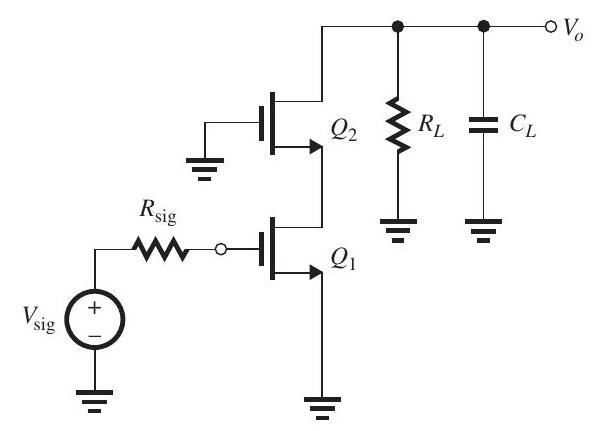
Figure 10.5.1
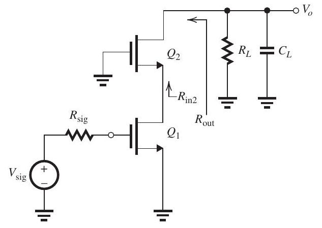
Figure 10.5.2
(a) The MOSFET in the common-source amplifier in Fig. 10.5.1, where the dc bias arrangement is not shown, is operating at and and has . The transistor capacitances are specified as and . Also, there is an additional capacitance between the output node and ground, . Find the overall de gain , the upper 3-dB frequency , and the gain-bandwidth product . To determine , use the method of open-circuit time constants and recall that the resistance seen by is given by , where .
(b) To increase , the common-source transistor is cascoded as shown in Fig. 10.5.2 (refer to Figure above), where the dc bias arrangement is not shown. For the same values of , and as in (a), assuming and are biased so that and , and for the capacitances of and to have the same values as specified in (a) above, find , and for the cascode amplifier. Recall that and .
In using the open-circuit time-constants method, adapt the formula given in (a) for to obtain . By what factor is increased?
Question
The MOSFET in the common-source amplifier in Fig. 10.6.1

Figure 10.6.1
has , and , and the total capacitance at the output node, , is .
(a) Find the value of the midband voltage gain.
(b) Use the method of short-circuit time constants to determine the lower 3-dB frequency, . Which capacitor dominates the determination of ?
(c) Use the method of open-circuit time constants to determine the upper 3-dB frequency, . Which capacitor dominates the determination of ?
Question
The amplifier in Fig. 10.7.1
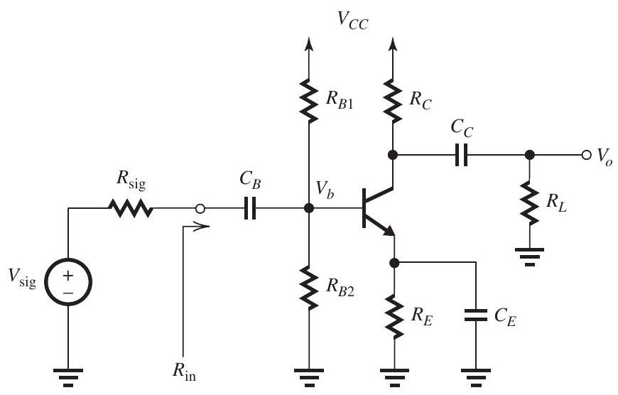
Figure 10.7.1
has , and .
(a) Assuming , find , and to operate the BJT at a dc bias point characterized by and . Design for and a voltage-divider current of .
(b) Find , and , assuming .
(c) At midband frequencies, find , , and , assuming .
(d) In the low-frequency band use the method of short-circuit time constants to obtain an estimate of the 3-dB frequency, .
(e) If and , use the Miller approximation to determine the input capacitance of the amplifier at high frequencies, and hence determine an estimate of the high-frequency frequency, .
Question
For the amplifier circuit in Fig. 10.8.1
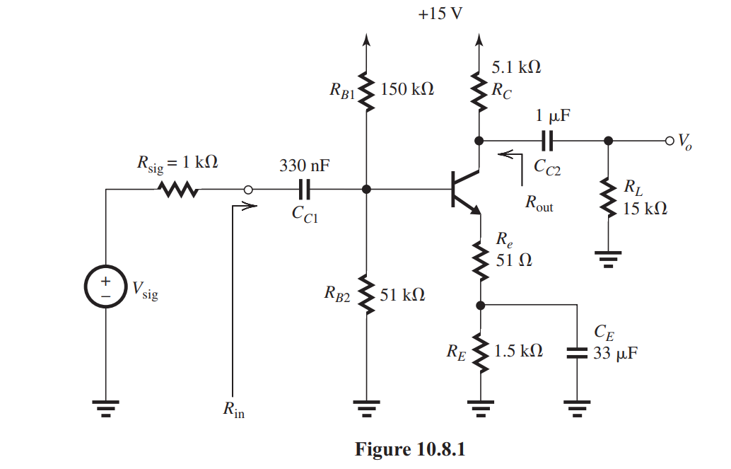
, assume that the BJT has and and neglect the Early effect.
(a) Find the dc bias current and the de collector voltage .
(b) Give the small-signal equivalent circuit together with values of all its components, utilizing the T model for the BJT.
(c) Find the input resistance .
(d) Find output resistance .
(e) Find the overall midband gain .
(f) Use the method of short-circuit time constants to obtain an estimate of the 3-dB frequency .
Question
The MOSFET in the common-source amplifier in Fig. 10.9.1
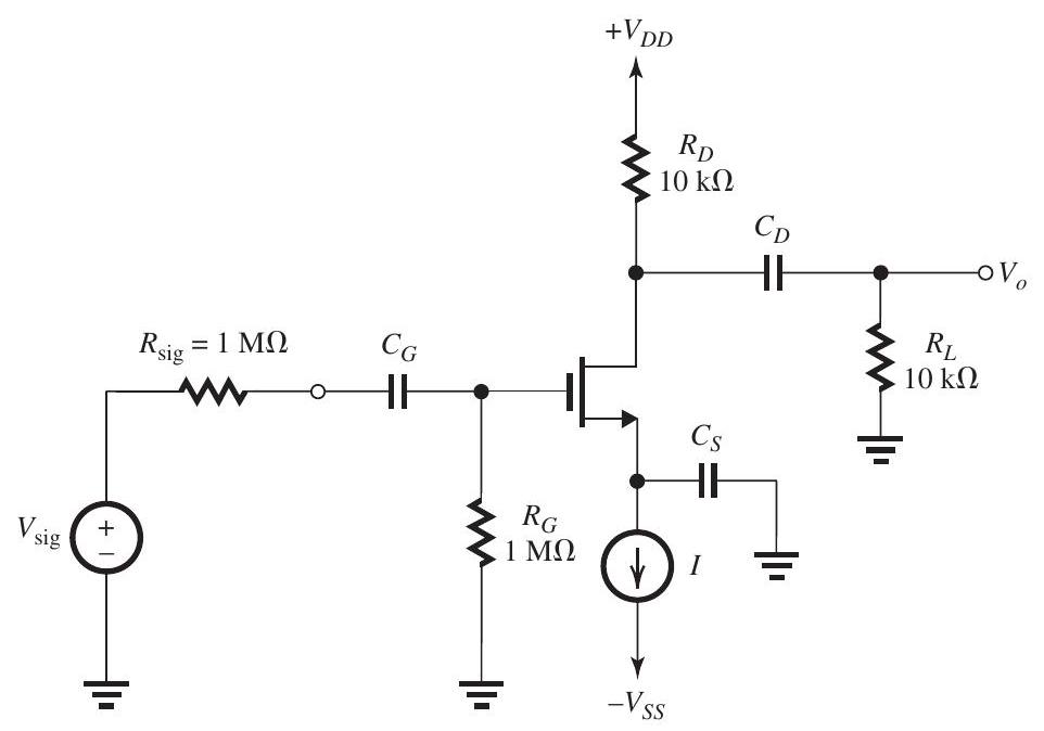
Figure 10.9.1
is operating at and has and . Channel-length modulation is negligibly small.
(a) Find the midband voltge gain in .
(b) Find the upper 3-dB frequency, .
(c) Find the value of that places the pole it introduces at .
(d) Find the value of that places the pole it introduces at
(e) Find the value of that places the pole it introduces at .
(f) Sketch and carefully label the Bode plot for the gain magnitude. Specify the lower 3-dB frequency, .
Question
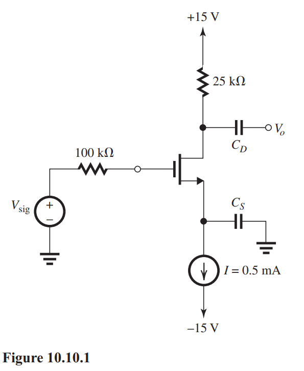
In the common-source amplifier shown in Fig. 10.10.1, the signal source has a zero average and provides de continuity to ground. The MOSFET has and .
(a) Find the value of at which the device is operating.
(b) Find the midband gain in and in dB.
(c) Find the value of that places the lower 3-dB frequency at .
(d) If and , find the value of the upper frequency, .
(e) It is desired to double by changing the value of (through changing the bias current ), find the required value of , the new value of the midband gain (in and in ), and the new value of .

Unlock Deck
Sign up to unlock the cards in this deck!
Unlock Deck
Unlock Deck
1/10
Play
Full screen (f)
Deck 6: Frequency Response
1
A common-source amplifier is fed from a signal source having a resistance and has a load resistance . The MOSFET has , and . The total capacitance between the output node and ground is .
(a) Find the midband gain.
(b) Use the method of open-circuit time constants to obtain an estimate of the upper 3-dB frequency, .
(a) Find the midband gain.
(b) Use the method of open-circuit time constants to obtain an estimate of the upper 3-dB frequency, .
Refer to Figure 10.1.1
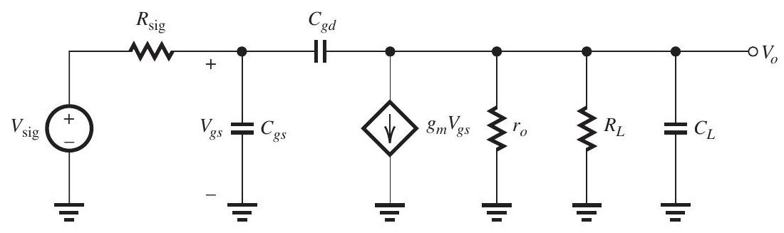
Figure 10.1.1
(a) At midband frequencies,
(b) Capacitor sees a resistance
Thus,
Capacitor sees a resistance
where
Thus,
and
Capacitor sees a resistance
Thus,
Finally,
and
Figure 10.1.1
(a) At midband frequencies,
(b) Capacitor sees a resistance
Thus,
Capacitor sees a resistance
where
Thus,
and
Capacitor sees a resistance
Thus,
Finally,
and
2
(a) Sketch the high-frequency equivalent circuit of a common-emitter amplifier that is fed with a voltage signal source having a resistance and that is loaded with a resistance . In addition to the internal capacitances of the BJT, and , there is a capacitance between the output node and ground.
(b) If the transistor is biased at and has , and , find the values of , and .
(c) Use the method of open-circuit time-constants to obtain an estimate for the upper 3-dB frequency, , for the case , and . Also, find the midband gain.
(b) If the transistor is biased at and has , and , find the values of , and .
(c) Use the method of open-circuit time-constants to obtain an estimate for the upper 3-dB frequency, , for the case , and . Also, find the midband gain.
(a) The high-frequency equivalent circuit is shown in Fig. 10.2.1 below.
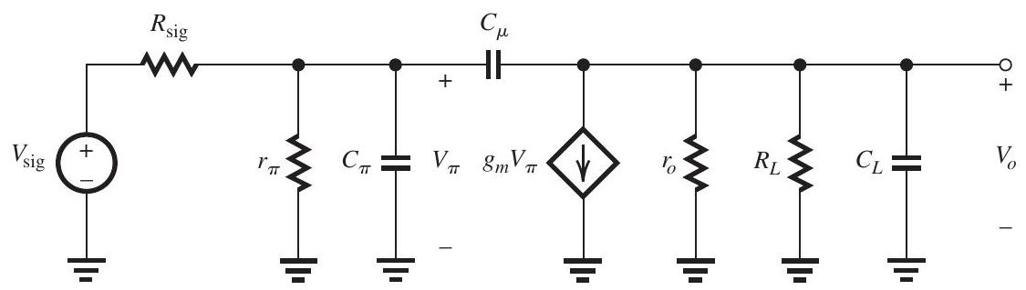
Figure 10.2.1
(b)
(c) Capacitor sees a resistance
Capacitor sees a resistance ,
where
Thus,
Capacitor sees a resistance ,
Now,
Figure 10.2.1
(b)
(c) Capacitor sees a resistance
Capacitor sees a resistance ,
where
Thus,
Capacitor sees a resistance ,
Now,
3
(a) An NMOS common-source amplifier with a simple PMOS current-source load has a total capacitance at the output node of . If the resistance of the signal source is very small, find the dc gain, the 3-dB frequency, and the gainbandwidth product, provided that and for each of the two transistors.
(b) If, in the circuit in (a), a cascode transistor is added to both the amplifier and the current-source load, find the new values of the gain, , and the gain-bandwidth product. Assume that all transistors have the same and as in (a) and that the total capacitance at the output node remains unchanged.
(b) If, in the circuit in (a), a cascode transistor is added to both the amplifier and the current-source load, find the new values of the gain, , and the gain-bandwidth product. Assume that all transistors have the same and as in (a) and that the total capacitance at the output node remains unchanged.
(a)
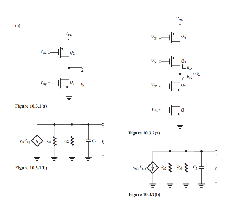
Figure 10.3.1 shows the amplifier together with its output equivalent circuit. The dc gain is given by
The 3-dB frequency is determined from the equivalent circuit as
(b)
Figure 10.3.2 shows the cascode amplifier together with its output equivalent circuit. The dc gain is given by
where
Thus,
The 3-dB frequency is determined from the equivalent circuit as
4
Figure 10.4.1
For the cascode amplifier in Fig. 10.4.1 (with the dc bias circuitry not shown), , , and . Investigate two designs, one that results in a de gain of and one that provides a dc gain of . For each case, find the required value of , the resulting 3 -dB frequency , and the gain-bandwidth product. Comment on the tradeoff between gain and bandwidth.
Unlock Deck
Unlock for access to all 10 flashcards in this deck.
Unlock Deck
k this deck
5
Figure 10.5.1
Figure 10.5.2
(a) The MOSFET in the common-source amplifier in Fig. 10.5.1, where the dc bias arrangement is not shown, is operating at and and has . The transistor capacitances are specified as and . Also, there is an additional capacitance between the output node and ground, . Find the overall de gain , the upper 3-dB frequency , and the gain-bandwidth product . To determine , use the method of open-circuit time constants and recall that the resistance seen by is given by , where .
(b) To increase , the common-source transistor is cascoded as shown in Fig. 10.5.2 (refer to Figure above), where the dc bias arrangement is not shown. For the same values of , and as in (a), assuming and are biased so that and , and for the capacitances of and to have the same values as specified in (a) above, find , and for the cascode amplifier. Recall that and .
In using the open-circuit time-constants method, adapt the formula given in (a) for to obtain . By what factor is increased?
Unlock Deck
Unlock for access to all 10 flashcards in this deck.
Unlock Deck
k this deck
6
The MOSFET in the common-source amplifier in Fig. 10.6.1
Figure 10.6.1
has , and , and the total capacitance at the output node, , is .
(a) Find the value of the midband voltage gain.
(b) Use the method of short-circuit time constants to determine the lower 3-dB frequency, . Which capacitor dominates the determination of ?
(c) Use the method of open-circuit time constants to determine the upper 3-dB frequency, . Which capacitor dominates the determination of ?
Unlock Deck
Unlock for access to all 10 flashcards in this deck.
Unlock Deck
k this deck
7
The amplifier in Fig. 10.7.1
Figure 10.7.1
has , and .
(a) Assuming , find , and to operate the BJT at a dc bias point characterized by and . Design for and a voltage-divider current of .
(b) Find , and , assuming .
(c) At midband frequencies, find , , and , assuming .
(d) In the low-frequency band use the method of short-circuit time constants to obtain an estimate of the 3-dB frequency, .
(e) If and , use the Miller approximation to determine the input capacitance of the amplifier at high frequencies, and hence determine an estimate of the high-frequency frequency, .
Unlock Deck
Unlock for access to all 10 flashcards in this deck.
Unlock Deck
k this deck
8
For the amplifier circuit in Fig. 10.8.1
, assume that the BJT has and and neglect the Early effect.
(a) Find the dc bias current and the de collector voltage .
(b) Give the small-signal equivalent circuit together with values of all its components, utilizing the T model for the BJT.
(c) Find the input resistance .
(d) Find output resistance .
(e) Find the overall midband gain .
(f) Use the method of short-circuit time constants to obtain an estimate of the 3-dB frequency .
Unlock Deck
Unlock for access to all 10 flashcards in this deck.
Unlock Deck
k this deck
9
The MOSFET in the common-source amplifier in Fig. 10.9.1
Figure 10.9.1
is operating at and has and . Channel-length modulation is negligibly small.
(a) Find the midband voltge gain in .
(b) Find the upper 3-dB frequency, .
(c) Find the value of that places the pole it introduces at .
(d) Find the value of that places the pole it introduces at
(e) Find the value of that places the pole it introduces at .
(f) Sketch and carefully label the Bode plot for the gain magnitude. Specify the lower 3-dB frequency, .
Unlock Deck
Unlock for access to all 10 flashcards in this deck.
Unlock Deck
k this deck
10
In the common-source amplifier shown in Fig. 10.10.1, the signal source has a zero average and provides de continuity to ground. The MOSFET has and .
(a) Find the value of at which the device is operating.
(b) Find the midband gain in and in dB.
(c) Find the value of that places the lower 3-dB frequency at .
(d) If and , find the value of the upper frequency, .
(e) It is desired to double by changing the value of (through changing the bias current ), find the required value of , the new value of the midband gain (in and in ), and the new value of .
Unlock Deck
Unlock for access to all 10 flashcards in this deck.
Unlock Deck
k this deck
Unlock Deck
Unlock for access to all 10 flashcards in this deck.


