Deck 7: Feedback
Full screen (f)
Question
Question
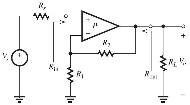
Figure 11.2.1
The series-shunt feedback amplifier shown in Fig. 11.2.1 utilizes a differential amplifier with a gain , input resistance , and output resistance . The feedback amplifier is fed with a signal source having a source resistance , and a load resistance is connected to the output terminal.
(a) If it is required to obtain a closed-loop gain that is ideally , what is the required feedback factor ? If , what value must have?
(b) Give the complete circuit and use it to determine , and .
(c) Find the actual value of realized.
(d) Find the input resistance of the feedback amplifier.
(e) Find the output resistance of the feedback amplifier.
(f) If, due to temperature variation, the gain changes by , what percentage change do you expect to have?
(g) If the high-frequency response of the amplifier is characterized by a drop of decade with a 3-dB frequency of , what do you expect the 3-dB frequency of the gain to be? At what frequency will the magnitude of become unity?
Question
The feedback amplifier shown in Fig. 11.3.1(a) employs the shunt-shunt feedback topology. To see this more clearly and to apply the feedback analysis method, convert the signal source together with the resistance to its Norton's equivalent circuit composed of current source together with a parallel resistance equal to . The amplifier has the equivalent circuit shown in Fig. 11.3.1(b). We wish to investigate the case for which , , and .
(a) Find the circuit and derive expressions for , and . Evaluate these expressions to determine , and .
(b) Find the circuit and derive an expression for . Find the value of .
(c) Find an expression for and its value.
(d) Find the value of the amount of feedback.
(e) Find the closed-loop gain and hence .
(f) Find the value of .
(g) Find the value of .
(h) If changes by , what is the resulting change in ?
Question
Figure 11.4.1
The series-shunt feedback amplifier shown in Fig. 11.4.1 uses a feedback network to sample the output voltage . Though the bias details are not shown, it is known that each of , , and is operating at a of and that their 's are very large.
(a) Give the circuit and find the value of .
(b) What do you estimate the approximate value of the closed-loop gain to be?
(c) Give the circuit and calculate the value of .
(d) Use the results of (a) and (c) to determine and compare the result to the value obtained in (b).
(e) Find the output resistance of the circuit.
(f) Find the output resistance of the closedloop amplifier.
(g) If the open-loop gain is found to have a dominant high-frequency pole at , what do you expect the upper 3-dB frequency of the closed-loop gain to be?
(h) If for some reason of decreases by , what is the corresponding percentage decrease in ?
Question
The feedback voltage amplifier in Fig. 11.5.1
Figure 11.5.1
utilizes the series-shunt feedback topology with the feedback network composed of and . The following component values are given: , and . The BJTs have , , and . The capacitors , , and are very large.
(a) Find values for , and so as to establish the following de conditions: , and . Hint: Do as many of your calculations as possible on Fig. 11.5.1 on the exam paper.
(b) Supply the circuit and find the values of , , and .
(c) Supply the circuit and find the value of .
(d) Find the closed-loop gain , the input resistance , and the output resistance
Question
Figure 11.6.1 (refer to Figure below)
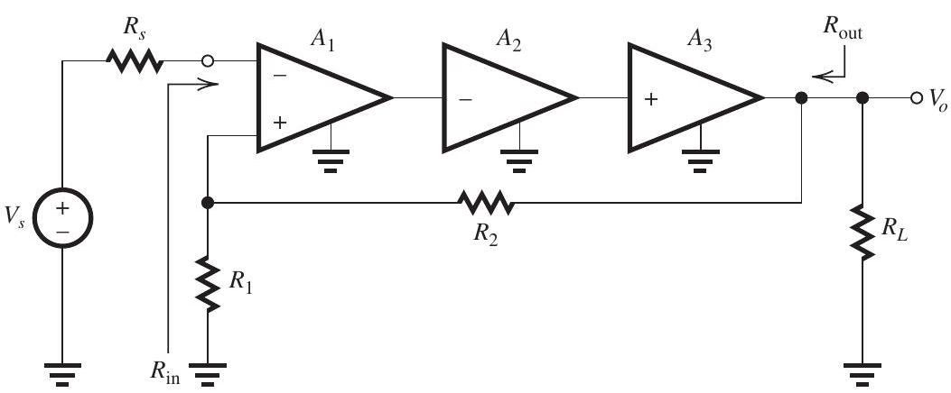
Figure 11.6.1
shows a feedback voltage amplifier in which the basic amplifier is composed of three cascaded stages having the following characteristics:
has a differential input resistance of , an open-circuit differential voltage gain of , and an output resistance of .
has an input resistance of , a shortcircuit tranconductance of , and an output resistance of . has an input resistance of , an opencircuit voltage gain of unity, and an output resistance of .
The feedback amplifier is fed with a signal source having and is connected to a load . The feedback network has and .
(a) Give the circuit and find the value of .
(b) Find and the amount of feedback.
(c) Find the closed-loop gain .
(d) Find the input resistance .
(e) Find the output resistance .
(f) If the high-frequency response of the openloop gain is dominated by a pole at , what is the upper 3-dB frequency of the closed-loop gain?
(g) If for some reason the gain of drops to half its nominal value, what is the percentage change in ?
Question
In the circuit of Fig. 11.7.1 (refer to Figure below), assume that coupling capacitors and are very large and thus act as perfect short circuits at
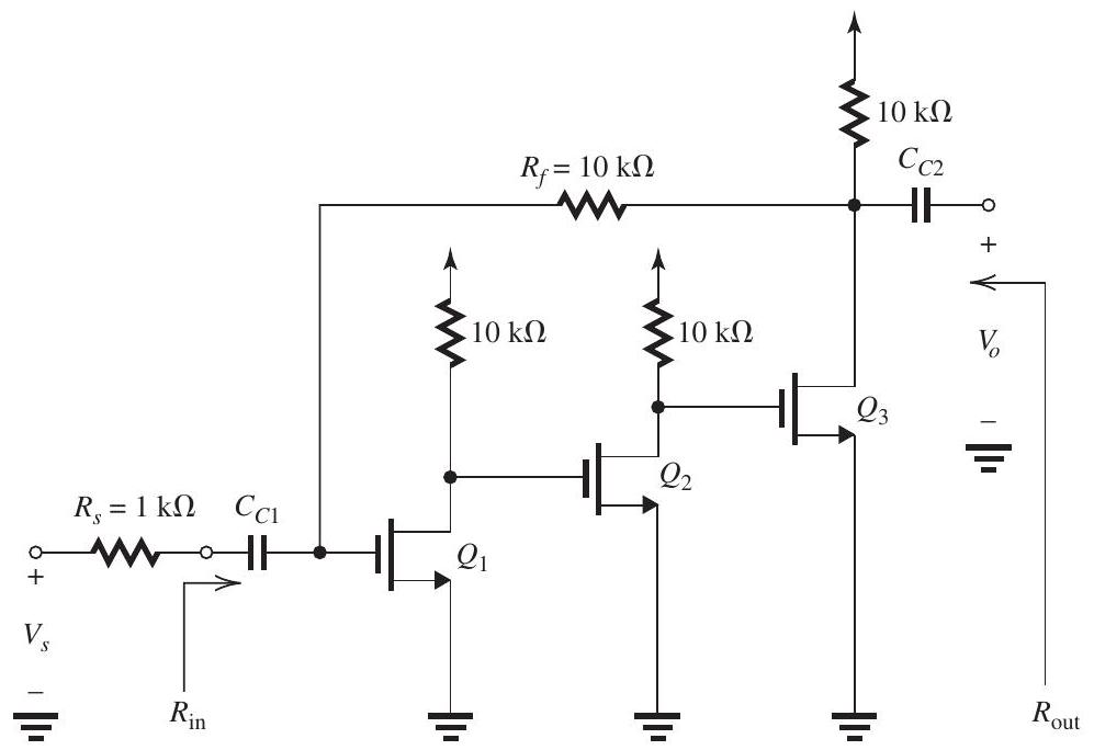
Figure 11.7.1
the frequencies of interest. Transistors , and are identical and are operating at identical dc bias conditions so that each has and .
(a) Replacing the signal source and with its Norton's equivalent circuit, show that this feedback amplifier utilizes the shunt-shunt feedback topology.
(b) Give the circuit and determine the value of .
(c) Give the ideal value of the closed-loop gain and hence of the voltage gain .
(d) Provide the circuit and determine the values of , and .
(e) Find the values of , and .
(f) Find the actual value of voltage gain realized and compare to the approximate value found in (c).
(g) Find the value of ,
(h) Find the value of .
(i) If is , find the magnitudes of the signals at the gates of , and and at the output (i.e., ).
Question
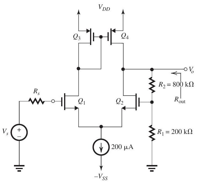
Figure 11.8.1
Figure 11.8.1 shows a MOS current-mirrorloaded differential amplifier with negative feedback applied through a voltage divider . Each of the four MOS transistors is operating at an overdrive voltage and has an Early voltage .
(a) Find expressions for and for the ideal value of the closed-loop gain . Hence, find the value of and the ideal value of .
(b) Give the circuit and expressions for and . Hence, find the values of the open-loop gain and the open-loop output resistances .
(c) Find the value of the closed-loop gain . Compare to the ideal value found in (a).
(d) Find the value of the output resistance .
Question
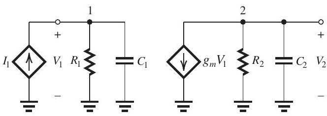
Figure 11.9.1
An op amp has a dc gain of and three real-axis poles with frequencies , , and . The op-amp internal circuit includes an amplifier stage having the equivalent circuit shown in Fig. 11.9.1, where , and . Furthermore, it is found that the input circuit of this stage is responsible for the pole at and that the output circuit is responsible for the pole at . It is required to frequency-compensate this op amp so that it becomes stable in closed-loop configurations with a closed-loop gain as low as unity.
(a) Sketch and clearly label a Bode plot for the op amp gain. Use a frequency axis that extends from to .
(b) If the frequency compensation is achieved by connecting a capacitor in parallel with , find the required value of and sketch the modified gain response on your Bode plot.
(c) If the frequency compensation is achieved by placing a capacitor in the feedback path of the amplifier stage in Fig. 11.9.1 -that is, between nodes 1 and 2 (Miller compensation)-find the required value of . Also, find the new frequencies of the poles and sketch the modified gain on your Bode plot.

Unlock Deck
Sign up to unlock the cards in this deck!
Unlock Deck
Unlock Deck
1/9
Play
Full screen (f)
Deck 7: Feedback
1
An amplifier with an open-loop gain of is connected in a feedback loop with the result that the closed-loop gain obtained is .
(a) Find the value of the amount of feedback, the loop gain, and the feedback factor.
(b) If the open-loop gain varies by , what is the corresponding variation of the closedloop gain?
(c) If the open-loop amplifier has 3-dB frequencies and , and the gain rolls off at the low and high frequency ends with a slope of , find the frequencies of the closed-loop gain and sketch the Bode magnitude plot of both the open-loop and closed-loop gains (on the same axes).
(a)
Thus,
Amount of feedback
Feedback factor
(b)
(c)
Figure 11.1.1
Sketches of the Bode plots for and are shown in Fig. 11.1.1.
2
Figure 11.2.1
The series-shunt feedback amplifier shown in Fig. 11.2.1 utilizes a differential amplifier with a gain , input resistance , and output resistance . The feedback amplifier is fed with a signal source having a source resistance , and a load resistance is connected to the output terminal.
(a) If it is required to obtain a closed-loop gain that is ideally , what is the required feedback factor ? If , what value must have?
(b) Give the complete circuit and use it to determine , and .
(c) Find the actual value of realized.
(d) Find the input resistance of the feedback amplifier.
(e) Find the output resistance of the feedback amplifier.
(f) If, due to temperature variation, the gain changes by , what percentage change do you expect to have?
(g) If the high-frequency response of the amplifier is characterized by a drop of decade with a 3-dB frequency of , what do you expect the 3-dB frequency of the gain to be? At what frequency will the magnitude of become unity?
![Figure 11.2.1 (a) For A_{f} to be ideally 10 \mathrm{~V} / \mathrm{V} , \beta=\frac{1}{A_{f}}=0.1 \mathrm{~V} / \mathrm{V} Figure 11.2.2 From the feedback network shown in Fig. 11.2.2, \begin{aligned} \beta & =\frac{R_{1}}{R_{1}+R_{2}} \\ 0.1 & =\frac{1}{1+R_{2}} \\ \Rightarrow R_{2} & =9 \mathrm{k} \Omega \end{aligned} (b) The A circuit is shown in Fig. 11.2.3 (refer to Figure below). Figure 11.2.3 \begin{aligned} A & =\frac{V_{o}}{V_{i}}=\frac{V_{1}}{V_{i}} \frac{V_{o}}{V_{1}} \\ & =\frac{R_{i d}}{R_{S}+R_{i d}+\left(R_{1} \| R_{2}\right)} \mu \frac{R_{L} \|\left(R_{1}+R_{2}\right)}{\left[R_{L} \|\left(R_{1}+R_{2}\right)\right]+r_{o}} \\ & =\frac{100}{10+100+(1 \| 9)} \times 10^{3} \times \frac{1 \|(1+9)}{[1 \|(1+9)]+1} \\ & =429.4 \mathrm{~V} / \mathrm{V} \\ R_{i} & =R_{S}+R_{i d}+\left(R_{1} \| R_{2}\right) \\ & =10+100+(1 \| 9) \\ & =110.9 \mathrm{k} \Omega \\ R_{O} & =R_{L}\left\|\left(R_{1}+R_{2}\right)\right\| r_{o} \\ & =1\|(1+9)\| 1 \\ & =476.2 \Omega \end{aligned} (c) \begin{aligned} A_{f} & =\frac{A}{1+A \beta} \\ & =\frac{429.4}{1+429.4 \times 0.1} \\ & =9.77 \mathrm{~V} / \mathrm{V} \end{aligned} (d) \begin{aligned} R_{i f} & =(1+A \beta) R_{i} \\ & =(1+429.4 \times 0.1) \times 110.9 \\ & =4.873 \mathrm{M} \Omega \\ R_{\text {in }} & =R_{i f}-R_{S}=4873-10 \\ & =4.863 \mathrm{M} \Omega \end{aligned} (e) \begin{aligned} R_{o f} & =\frac{R_{o}}{1+A \beta} \\ & =\frac{476.2}{43.94}=10.84 \Omega \end{aligned} Since \begin{aligned} \frac{1}{R_{\text {of }}} & =\frac{1}{R_{L}}+\frac{1}{R_{\mathrm{out}}} \\ \Rightarrow R_{\mathrm{out}} & =10.96 \Omega \end{aligned} (f) \begin{aligned} \frac{\triangle \mu}{\mu} & =10 \% \\ \Rightarrow \frac{\triangle A}{A} & =10 \% \\ \Rightarrow \frac{\triangle A_{f}}{A_{f}} & =\frac{\triangle A / A}{1+A \beta} \\ & =\frac{10}{43.94}=0.23 \% \end{aligned} (g) \begin{aligned} f_{H f} & =(1+A \beta) f_{H} \\ & =43.94 \times 10 \\ & =439.4 \mathrm{kHz} \end{aligned} \left|A_{f}\right| reaches unity at \begin{aligned} f_{t} & =\left|A_{f}\right| \times f_{H f}=9.77 \times 439.4 \\ & =4.29 \mathrm{MHz} \end{aligned}](https://d2lvgg3v3hfg70.cloudfront.net/TBO1243/11eeb9e9_cbc0_9b81_9342_17d539ce2c4e_TBO1243_00.jpg)
Figure 11.2.1
(a) For to be ideally ,
![Figure 11.2.1 (a) For A_{f} to be ideally 10 \mathrm{~V} / \mathrm{V} , \beta=\frac{1}{A_{f}}=0.1 \mathrm{~V} / \mathrm{V} Figure 11.2.2 From the feedback network shown in Fig. 11.2.2, \begin{aligned} \beta & =\frac{R_{1}}{R_{1}+R_{2}} \\ 0.1 & =\frac{1}{1+R_{2}} \\ \Rightarrow R_{2} & =9 \mathrm{k} \Omega \end{aligned} (b) The A circuit is shown in Fig. 11.2.3 (refer to Figure below). Figure 11.2.3 \begin{aligned} A & =\frac{V_{o}}{V_{i}}=\frac{V_{1}}{V_{i}} \frac{V_{o}}{V_{1}} \\ & =\frac{R_{i d}}{R_{S}+R_{i d}+\left(R_{1} \| R_{2}\right)} \mu \frac{R_{L} \|\left(R_{1}+R_{2}\right)}{\left[R_{L} \|\left(R_{1}+R_{2}\right)\right]+r_{o}} \\ & =\frac{100}{10+100+(1 \| 9)} \times 10^{3} \times \frac{1 \|(1+9)}{[1 \|(1+9)]+1} \\ & =429.4 \mathrm{~V} / \mathrm{V} \\ R_{i} & =R_{S}+R_{i d}+\left(R_{1} \| R_{2}\right) \\ & =10+100+(1 \| 9) \\ & =110.9 \mathrm{k} \Omega \\ R_{O} & =R_{L}\left\|\left(R_{1}+R_{2}\right)\right\| r_{o} \\ & =1\|(1+9)\| 1 \\ & =476.2 \Omega \end{aligned} (c) \begin{aligned} A_{f} & =\frac{A}{1+A \beta} \\ & =\frac{429.4}{1+429.4 \times 0.1} \\ & =9.77 \mathrm{~V} / \mathrm{V} \end{aligned} (d) \begin{aligned} R_{i f} & =(1+A \beta) R_{i} \\ & =(1+429.4 \times 0.1) \times 110.9 \\ & =4.873 \mathrm{M} \Omega \\ R_{\text {in }} & =R_{i f}-R_{S}=4873-10 \\ & =4.863 \mathrm{M} \Omega \end{aligned} (e) \begin{aligned} R_{o f} & =\frac{R_{o}}{1+A \beta} \\ & =\frac{476.2}{43.94}=10.84 \Omega \end{aligned} Since \begin{aligned} \frac{1}{R_{\text {of }}} & =\frac{1}{R_{L}}+\frac{1}{R_{\mathrm{out}}} \\ \Rightarrow R_{\mathrm{out}} & =10.96 \Omega \end{aligned} (f) \begin{aligned} \frac{\triangle \mu}{\mu} & =10 \% \\ \Rightarrow \frac{\triangle A}{A} & =10 \% \\ \Rightarrow \frac{\triangle A_{f}}{A_{f}} & =\frac{\triangle A / A}{1+A \beta} \\ & =\frac{10}{43.94}=0.23 \% \end{aligned} (g) \begin{aligned} f_{H f} & =(1+A \beta) f_{H} \\ & =43.94 \times 10 \\ & =439.4 \mathrm{kHz} \end{aligned} \left|A_{f}\right| reaches unity at \begin{aligned} f_{t} & =\left|A_{f}\right| \times f_{H f}=9.77 \times 439.4 \\ & =4.29 \mathrm{MHz} \end{aligned}](https://d2lvgg3v3hfg70.cloudfront.net/TBO1243/11eeb9e9_cbc0_9b82_9342_b3195f7dde76_TBO1243_00.jpg)
Figure 11.2.2
From the feedback network shown in Fig. 11.2.2,
(b) The circuit is shown in Fig. 11.2.3 (refer to Figure below).
![Figure 11.2.1 (a) For A_{f} to be ideally 10 \mathrm{~V} / \mathrm{V} , \beta=\frac{1}{A_{f}}=0.1 \mathrm{~V} / \mathrm{V} Figure 11.2.2 From the feedback network shown in Fig. 11.2.2, \begin{aligned} \beta & =\frac{R_{1}}{R_{1}+R_{2}} \\ 0.1 & =\frac{1}{1+R_{2}} \\ \Rightarrow R_{2} & =9 \mathrm{k} \Omega \end{aligned} (b) The A circuit is shown in Fig. 11.2.3 (refer to Figure below). Figure 11.2.3 \begin{aligned} A & =\frac{V_{o}}{V_{i}}=\frac{V_{1}}{V_{i}} \frac{V_{o}}{V_{1}} \\ & =\frac{R_{i d}}{R_{S}+R_{i d}+\left(R_{1} \| R_{2}\right)} \mu \frac{R_{L} \|\left(R_{1}+R_{2}\right)}{\left[R_{L} \|\left(R_{1}+R_{2}\right)\right]+r_{o}} \\ & =\frac{100}{10+100+(1 \| 9)} \times 10^{3} \times \frac{1 \|(1+9)}{[1 \|(1+9)]+1} \\ & =429.4 \mathrm{~V} / \mathrm{V} \\ R_{i} & =R_{S}+R_{i d}+\left(R_{1} \| R_{2}\right) \\ & =10+100+(1 \| 9) \\ & =110.9 \mathrm{k} \Omega \\ R_{O} & =R_{L}\left\|\left(R_{1}+R_{2}\right)\right\| r_{o} \\ & =1\|(1+9)\| 1 \\ & =476.2 \Omega \end{aligned} (c) \begin{aligned} A_{f} & =\frac{A}{1+A \beta} \\ & =\frac{429.4}{1+429.4 \times 0.1} \\ & =9.77 \mathrm{~V} / \mathrm{V} \end{aligned} (d) \begin{aligned} R_{i f} & =(1+A \beta) R_{i} \\ & =(1+429.4 \times 0.1) \times 110.9 \\ & =4.873 \mathrm{M} \Omega \\ R_{\text {in }} & =R_{i f}-R_{S}=4873-10 \\ & =4.863 \mathrm{M} \Omega \end{aligned} (e) \begin{aligned} R_{o f} & =\frac{R_{o}}{1+A \beta} \\ & =\frac{476.2}{43.94}=10.84 \Omega \end{aligned} Since \begin{aligned} \frac{1}{R_{\text {of }}} & =\frac{1}{R_{L}}+\frac{1}{R_{\mathrm{out}}} \\ \Rightarrow R_{\mathrm{out}} & =10.96 \Omega \end{aligned} (f) \begin{aligned} \frac{\triangle \mu}{\mu} & =10 \% \\ \Rightarrow \frac{\triangle A}{A} & =10 \% \\ \Rightarrow \frac{\triangle A_{f}}{A_{f}} & =\frac{\triangle A / A}{1+A \beta} \\ & =\frac{10}{43.94}=0.23 \% \end{aligned} (g) \begin{aligned} f_{H f} & =(1+A \beta) f_{H} \\ & =43.94 \times 10 \\ & =439.4 \mathrm{kHz} \end{aligned} \left|A_{f}\right| reaches unity at \begin{aligned} f_{t} & =\left|A_{f}\right| \times f_{H f}=9.77 \times 439.4 \\ & =4.29 \mathrm{MHz} \end{aligned}](https://d2lvgg3v3hfg70.cloudfront.net/TBO1243/11eeb9e9_cbc0_9b83_9342_07d90b862c1e_TBO1243_00.jpg) Figure 11.2.3
Figure 11.2.3(c)
(d)
(e)
Since
(f)
(g)
reaches unity at
3
The feedback amplifier shown in Fig. 11.3.1(a) employs the shunt-shunt feedback topology. To see this more clearly and to apply the feedback analysis method, convert the signal source together with the resistance to its Norton's equivalent circuit composed of current source together with a parallel resistance equal to . The amplifier has the equivalent circuit shown in Fig. 11.3.1(b). We wish to investigate the case for which , , and .
(a) Find the circuit and derive expressions for , and . Evaluate these expressions to determine , and .
(b) Find the circuit and derive an expression for . Find the value of .
(c) Find an expression for and its value.
(d) Find the value of the amount of feedback.
(e) Find the closed-loop gain and hence .
(f) Find the value of .
(g) Find the value of .
(h) If changes by , what is the resulting change in ?
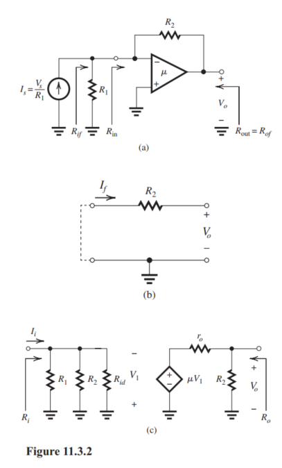
(a) Figure 11.3.2(a) shows the shunt-shunt feedback amplifier (transresistance amplifier) with and converted to the Norton form. The circuit is shown in Fig. 11.3.2(b) and the circuit is shown in Fig. 11.3.2(c). From the latter,
Thus,
(b) The circuit is shown in Fig. 11.3.2(b).
(c)
(d)
(e)
(f)
But,
(g)
(h)
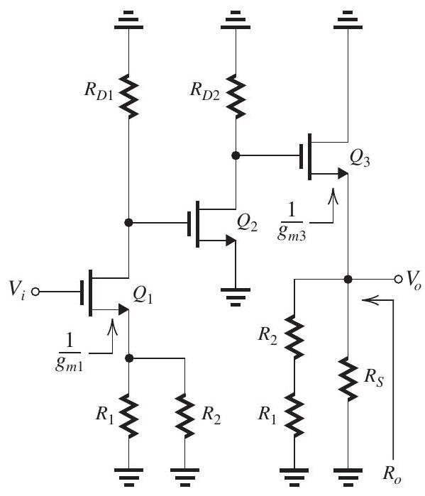
Figure 11.4.3
4
Figure 11.4.1
The series-shunt feedback amplifier shown in Fig. 11.4.1 uses a feedback network to sample the output voltage . Though the bias details are not shown, it is known that each of , , and is operating at a of and that their 's are very large.
(a) Give the circuit and find the value of .
(b) What do you estimate the approximate value of the closed-loop gain to be?
(c) Give the circuit and calculate the value of .
(d) Use the results of (a) and (c) to determine and compare the result to the value obtained in (b).
(e) Find the output resistance of the circuit.
(f) Find the output resistance of the closedloop amplifier.
(g) If the open-loop gain is found to have a dominant high-frequency pole at , what do you expect the upper 3-dB frequency of the closed-loop gain to be?
(h) If for some reason of decreases by , what is the corresponding percentage decrease in ?
Unlock Deck
Unlock for access to all 9 flashcards in this deck.
Unlock Deck
k this deck
5
The feedback voltage amplifier in Fig. 11.5.1
Figure 11.5.1
utilizes the series-shunt feedback topology with the feedback network composed of and . The following component values are given: , and . The BJTs have , , and . The capacitors , , and are very large.
(a) Find values for , and so as to establish the following de conditions: , and . Hint: Do as many of your calculations as possible on Fig. 11.5.1 on the exam paper.
(b) Supply the circuit and find the values of , , and .
(c) Supply the circuit and find the value of .
(d) Find the closed-loop gain , the input resistance , and the output resistance
Figure 11.5.1
utilizes the series-shunt feedback topology with the feedback network composed of and . The following component values are given: , and . The BJTs have , , and . The capacitors , , and are very large.
(a) Find values for , and so as to establish the following de conditions: , and . Hint: Do as many of your calculations as possible on Fig. 11.5.1 on the exam paper.
(b) Supply the circuit and find the values of , , and .
(c) Supply the circuit and find the value of .
(d) Find the closed-loop gain , the input resistance , and the output resistance
Unlock Deck
Unlock for access to all 9 flashcards in this deck.
Unlock Deck
k this deck
6
Figure 11.6.1 (refer to Figure below)
Figure 11.6.1
shows a feedback voltage amplifier in which the basic amplifier is composed of three cascaded stages having the following characteristics:
has a differential input resistance of , an open-circuit differential voltage gain of , and an output resistance of .
has an input resistance of , a shortcircuit tranconductance of , and an output resistance of . has an input resistance of , an opencircuit voltage gain of unity, and an output resistance of .
The feedback amplifier is fed with a signal source having and is connected to a load . The feedback network has and .
(a) Give the circuit and find the value of .
(b) Find and the amount of feedback.
(c) Find the closed-loop gain .
(d) Find the input resistance .
(e) Find the output resistance .
(f) If the high-frequency response of the openloop gain is dominated by a pole at , what is the upper 3-dB frequency of the closed-loop gain?
(g) If for some reason the gain of drops to half its nominal value, what is the percentage change in ?
Unlock Deck
Unlock for access to all 9 flashcards in this deck.
Unlock Deck
k this deck
7
In the circuit of Fig. 11.7.1 (refer to Figure below), assume that coupling capacitors and are very large and thus act as perfect short circuits at
Figure 11.7.1
the frequencies of interest. Transistors , and are identical and are operating at identical dc bias conditions so that each has and .
(a) Replacing the signal source and with its Norton's equivalent circuit, show that this feedback amplifier utilizes the shunt-shunt feedback topology.
(b) Give the circuit and determine the value of .
(c) Give the ideal value of the closed-loop gain and hence of the voltage gain .
(d) Provide the circuit and determine the values of , and .
(e) Find the values of , and .
(f) Find the actual value of voltage gain realized and compare to the approximate value found in (c).
(g) Find the value of ,
(h) Find the value of .
(i) If is , find the magnitudes of the signals at the gates of , and and at the output (i.e., ).
Unlock Deck
Unlock for access to all 9 flashcards in this deck.
Unlock Deck
k this deck
8
Figure 11.8.1
Figure 11.8.1 shows a MOS current-mirrorloaded differential amplifier with negative feedback applied through a voltage divider . Each of the four MOS transistors is operating at an overdrive voltage and has an Early voltage .
(a) Find expressions for and for the ideal value of the closed-loop gain . Hence, find the value of and the ideal value of .
(b) Give the circuit and expressions for and . Hence, find the values of the open-loop gain and the open-loop output resistances .
(c) Find the value of the closed-loop gain . Compare to the ideal value found in (a).
(d) Find the value of the output resistance .
Unlock Deck
Unlock for access to all 9 flashcards in this deck.
Unlock Deck
k this deck
9
Figure 11.9.1
An op amp has a dc gain of and three real-axis poles with frequencies , , and . The op-amp internal circuit includes an amplifier stage having the equivalent circuit shown in Fig. 11.9.1, where , and . Furthermore, it is found that the input circuit of this stage is responsible for the pole at and that the output circuit is responsible for the pole at . It is required to frequency-compensate this op amp so that it becomes stable in closed-loop configurations with a closed-loop gain as low as unity.
(a) Sketch and clearly label a Bode plot for the op amp gain. Use a frequency axis that extends from to .
(b) If the frequency compensation is achieved by connecting a capacitor in parallel with , find the required value of and sketch the modified gain response on your Bode plot.
(c) If the frequency compensation is achieved by placing a capacitor in the feedback path of the amplifier stage in Fig. 11.9.1 -that is, between nodes 1 and 2 (Miller compensation)-find the required value of . Also, find the new frequencies of the poles and sketch the modified gain on your Bode plot.
Unlock Deck
Unlock for access to all 9 flashcards in this deck.
Unlock Deck
k this deck
Unlock Deck
Unlock for access to all 9 flashcards in this deck.


