Deck 8: Operational Amplifier Circuits, Filters, Oscillators and CMOS Digital Logic Circuits
Full screen (f)
Question
Figure 13.1.1
For the two-stage CMOS op amp shown in Fig. 13.1.1, all transistors have the same channel length , and . Transistors , and are matched; and are matched; and and are matched.
Parts (a) to (d) below deal with de bias calculations, and in these, assume the two input terminals are grounded and neglect the Early effect.
(a) Find the values of , and so that a dc voltage of appears at the gate of and dc current of flows in the drains of and .
(b) Find and that will result in each of and operating with an overdrive voltage of .
(c) Find and that will result in a dc voltage of at the gates of and .
(d) What de voltage appears at the gate of ? Find that will result in zero de current flowing through the output terminal of the amplifier.
(e) Find the input common-mode range.
(f) Find the allowable range of the output signal swing.
(g) Find the values of , and .
(h) Find the value of the differential gain of the first stage, .
(i) Recalling that the common-mode gain of the current-mirror-loaded differential amplifier is given by , where is the output resistance of , find , the commonmode gain, and the CMRR in .
(j) Find , and .
(k) Find the voltage gain of the second stage, .
(1) Find the overall differential voltage gain and the output resistance .
(m) If the feedback loop around the amplifier is closed by connecting the output terminal to the inverting input terminal, find the closedloop gain (between the non-inverting input terminal and the output) specified to four significant digits and determine the closed-loop output resistance .
(n) If, alternatively, the feedback loop around the op amp is closed by connecting the feedback network shown in Fig. 13.1.2, find the new values of and and the values of , the closed-loop gain , and the output resistance .
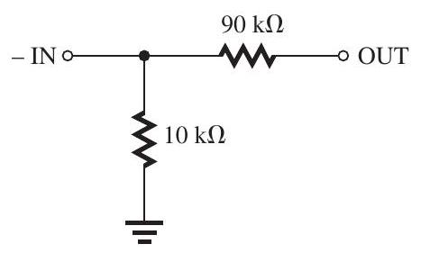
Figure 13.1.2
Question
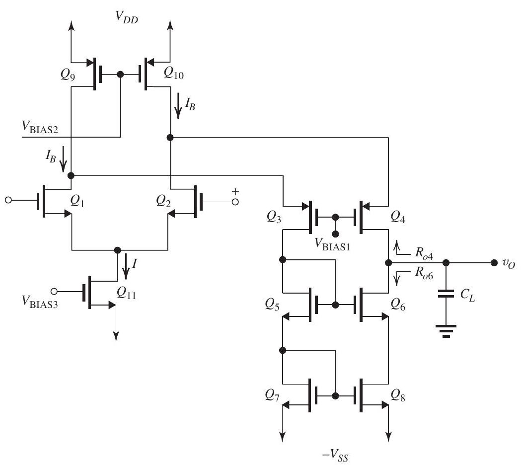
Figure 13.2.1
It is required to design the folded-cascode op amp shown in Fig. 13.2.1. Let and , and assume that for all transistors, . Design so that the power dissipated in the circuit (with no input signal applied) is , and so that each of and is operating at a current four times that at which each of and is operating. Also, design so that all transistors operate at .
(a) Show that the current drawn from each of the two power supplies is , and hence find and that result in the circuit operating at its specified power dissipation.
(b) Find the dc current at which each of to is operating. Present your results in a table.
(c) Find the input common-mode range.
(d) Find the required values of , and that result in the maximum allowable value of to be as high as possible.
(e) Find the allowable range of .
(f) Find the overall transconductance .
(g) Find the output resistance .
(h) Find the low-frequency voltage gain.
(i) If the amplifier at its output is modeled by a controlled current-source (where is the differential input voltage) feeding the output resistance and the total capacitance at the output node , find the value of that results in the amplifier having a unity-gain bandwidth of . Assume that the dominant pole is that formed at the output.
Question
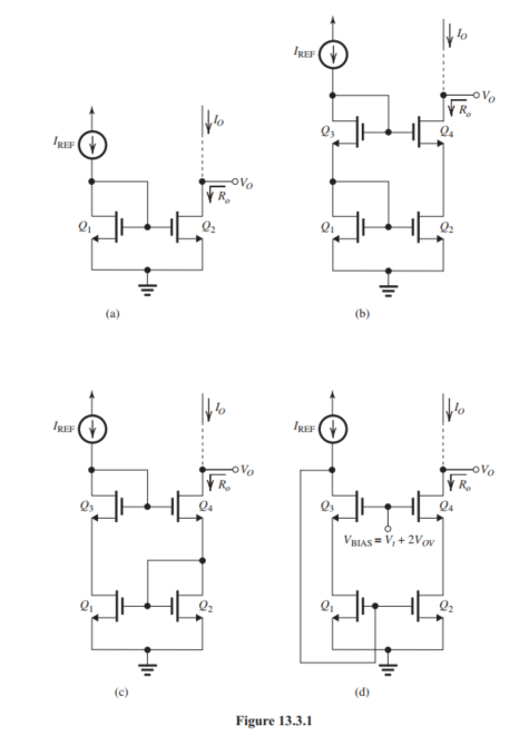
In the current-mirror circuits in Fig. 13.3.1, all transistors are operating at the same current and have the same and the same . Identify each current-mirror (i.e., give its name) and give its output resistance in terms of , and . Also, give the minimum voltage each mirror requires to operate properly. Give in terms of and .
Question
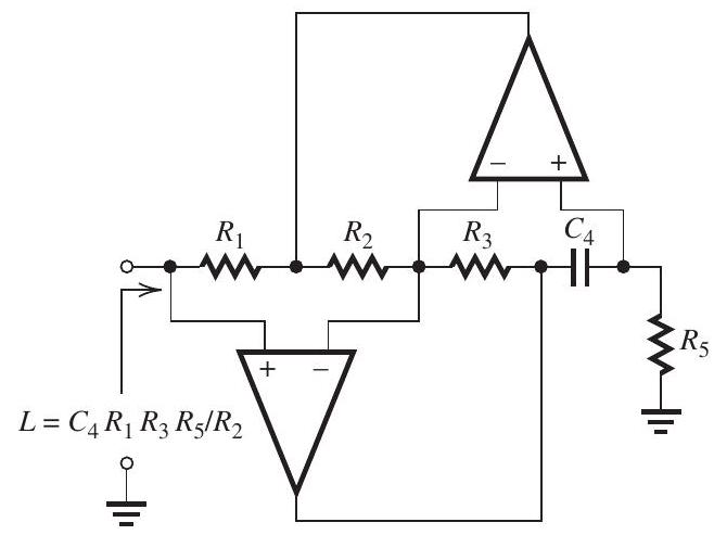
Figure 14.1.1
It is required to design a fifth-order Butterworth low-pass filter with a de gain of unity, a passband edge of , and a maximum deviation in the passband transmission of (i.e., ).
(a) Find the transfer function and give and of each of the two pairs of complex-conjugate poles. Also, specify the frequency of the real pole.
(b) Provide a complete circuit realization of the filter as a cascade of two second-order sections and a first-order section. For the second-order sections, use realizations based on the inductancesimulation circuit of Fig. 14.1.1. For the first-order section, use an op amp-RC circuit. Design so that all capacitors are equal to and as many of the resistors as possible are equal. Give the complete circuit and specify the values of all resistors.
(c) What is the attenuation achieved at the stopband edge, ?
Question
In the cross-coupled oscillator circuit shown in Fig. 15.1.1, represents the loss of each inductor. Each transistor is operating at a transconductance and has an output resistance . Find the oscillation frequency and explain why the circuit oscillates at this frequency. Also, derive an expression for the minimum value of needed to obtain sustained oscillations.
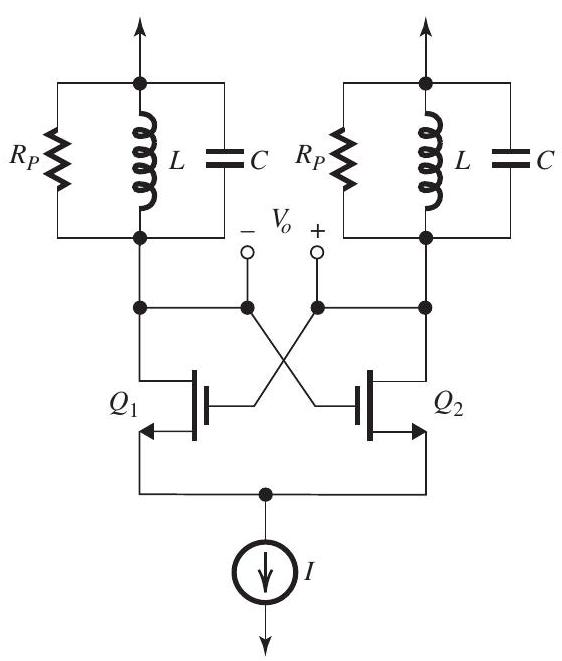
Figure 15.1.1
Figure 15.1.1
Question
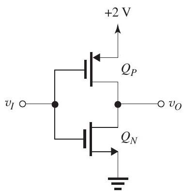
Figure 16.1.1
(a) For the CMOS inverter in Fig. 16.1.1, and have and . Sketch and clearly label the VTC versus and give values for the noise margins and . What is the output resistance when ?
(b) Provide the CMOS realization of the logic function.
Question
The CMOS inverter shown in Fig. 16.2.1 has and is fabricated in a process for which , and . For this problem, neglect the Early effect. Both and use the minimum channel length allowed. For .
(a) Find the dimensions that must have in order for the inverter switching to occur at .
(b) What are the noise margins of the inverter?
(c) What current flows in and at the switching point?
(d) For , what is the maximum current that can sink while is limited to ?
Question
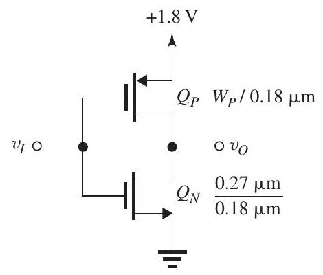
Figure 16.3.1
The CMOS inverter shown in Fig. 16.3.1 is fabricated in a technology having , , and .
(a) Find to obtain matched transistors.
(b) For , find the maximum load current that the inverter can sink while is not exceeding .
Question
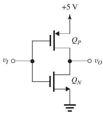
Figure 16.4.1
The transistors in the CMOS inverter in Fig. 16.4.1 have , and .
(a) What is the value of the gate threshold?
(b) For , what is the resistance between the output terminal and the supply? If a resistance is connected between the output terminal and ground, what will be?

Unlock Deck
Sign up to unlock the cards in this deck!
Unlock Deck
Unlock Deck
1/9
Play
Full screen (f)
Deck 8: Operational Amplifier Circuits, Filters, Oscillators and CMOS Digital Logic Circuits
1
Figure 13.1.1
For the two-stage CMOS op amp shown in Fig. 13.1.1, all transistors have the same channel length , and . Transistors , and are matched; and are matched; and and are matched.
Parts (a) to (d) below deal with de bias calculations, and in these, assume the two input terminals are grounded and neglect the Early effect.
(a) Find the values of , and so that a dc voltage of appears at the gate of and dc current of flows in the drains of and .
(b) Find and that will result in each of and operating with an overdrive voltage of .
(c) Find and that will result in a dc voltage of at the gates of and .
(d) What de voltage appears at the gate of ? Find that will result in zero de current flowing through the output terminal of the amplifier.
(e) Find the input common-mode range.
(f) Find the allowable range of the output signal swing.
(g) Find the values of , and .
(h) Find the value of the differential gain of the first stage, .
(i) Recalling that the common-mode gain of the current-mirror-loaded differential amplifier is given by , where is the output resistance of , find , the commonmode gain, and the CMRR in .
(j) Find , and .
(k) Find the voltage gain of the second stage, .
(1) Find the overall differential voltage gain and the output resistance .
(m) If the feedback loop around the amplifier is closed by connecting the output terminal to the inverting input terminal, find the closedloop gain (between the non-inverting input terminal and the output) specified to four significant digits and determine the closed-loop output resistance .
(n) If, alternatively, the feedback loop around the op amp is closed by connecting the feedback network shown in Fig. 13.1.2, find the new values of and and the values of , the closed-loop gain , and the output resistance .
Figure 13.1.2
![Figure 13.1.1 (a) With V_{G 8}=V_{G 7}=V_{G 5}=-1.5 \mathrm{~V} , V_{G S 5}=V_{G S 7}=V_{G S 8}=1 \mathrm{~V} Thus, each of Q_{5}, Q_{7} , and Q_{8} is operating at V_{O V}=1-0.6=0.4 \mathrm{~V} To obtain I_{D 1}=I_{D 2}=50 \mu \mathrm{A} , we must establish I_{D 5}=100 \mu \mathrm{A} Thus, I_{\mathrm{REF}}=I_{D 8}=I_{D 5}=100 \mu \mathrm{A} But \begin{aligned} I_{\mathrm{REF}} & =\frac{V_{D D}-V_{G 8}}{R} \\ 0.1 & =\frac{2.5-(-1.5)}{R} \\ \Rightarrow R & =40 \mathrm{k} \Omega \end{aligned} For each of Q_{5}, Q_{7} , and Q_{8} , \begin{aligned} I_{D} & =\frac{1}{2}\left(\mu_{n} C_{O x}\right)\left(\frac{W}{L}\right) V_{O V}^{2} \\ 100 & =\frac{1}{2} \times 200 \times\left(\frac{W}{L}\right) \times 0.4^{2} \\ \Rightarrow \frac{W}{L} & =6.25 \end{aligned} Thus, W_{5}=W_{7}=W_{8}=6.25 \times 0.8=5 \mu \mathrm{m} . (b) For each of Q_{1} and Q_{2} , \begin{aligned} I_{D} & =\frac{1}{2}\left(\mu_{n} C_{O x}\right)\left(\frac{W_{1,2}}{L}\right) V_{O V 1,2}^{2} \\ 50 & =\frac{1}{2} \times 200 \times \frac{W_{1,2}}{L} \times 0.2^{2} \\ \Rightarrow \frac{W_{1,2}}{L} & =12.5 \\ \Rightarrow W_{1} & =W_{2}=12.5 \times 0.8=10 \mu \mathrm{m} \end{aligned} (c) \begin{aligned} V_{G 3}=V_{G 4} & =+1.5 \mathrm{~V} \\ \Rightarrow V_{S G 3}=V_{S G 4} & =1 \mathrm{~V} \\ \Rightarrow\left|V_{O V 3,4}\right| & =0.4 \mathrm{~V} \end{aligned} For Q_{3} and Q_{4} , \begin{aligned} I_{D} & =\frac{1}{2}\left(\mu_{p} C_{O x}\right)\left(\frac{W_{3,4}}{L}\right)\left|V_{O V 3,4}\right|^{2} \\ 50 & =\frac{1}{2} \times 100 \times \frac{W_{3,4}}{L} \times 0.4^{2} \\ \Rightarrow \frac{W_{3,4}}{L} & =6.25 \mu \mathrm{m} \\ \Rightarrow W_{3} & =W_{4}=6.25 \times 0.8=5 \mu \mathrm{m} \end{aligned} (d) For matched conditions, \begin{aligned} V_{D 4} & =V_{G 4}=+1.5 \mathrm{~V} \\ \Rightarrow V_{G 6} & =+1.5 \mathrm{~V} \\ V_{S G 6} & =1 \mathrm{~V} \end{aligned} Thus, Q_{6} will be operating at \left|V_{O V}\right|=0.4 \mathrm{~V} . For zero dc output current, I_{D 6}=I_{D 7}=100 \mu \mathrm{A} Thus, \begin{aligned} 100 & =\frac{1}{2}\left(\mu_{p} C_{o x}\right)\left(\frac{W_{6}}{L}\right)\left|V_{O V 6}\right|^{2} \\ 100 & =\frac{1}{2} \times 100 \times \frac{W_{6}}{L} \times 0.4^{2} \\ \Rightarrow \frac{W_{6}}{L} & =12.5 \\ \Rightarrow W_{6} & =12.5 \times 0.8=10 \mu \mathrm{m} \end{aligned} (e) \begin{aligned} V_{I C M \max } & =V_{D 1}+V_{t n}=+1.5+0.6=+2.1 \mathrm{~V} \\ V_{I C M \min } & =-V_{S S}+V_{O V 5}+V_{G S 1} \\ & =-2.5+0.4+(0.6+0.2)=-1.3 \mathrm{~V} \end{aligned} Thus, -1.3 \mathrm{~V} \leq V_{I C M} \leq+2.1 \mathrm{~V} (f) \begin{aligned} v_{O \max } & =V_{D D}-\left|V_{O V 6}\right| \\ & =+2.5-0.4=+2.1 \mathrm{~V} \\ v_{O \min } & =-V_{S S}+V_{O V 7} \\ & =-2.5+0.4=-2.1 \mathrm{~V} \end{aligned} Thus, -2.1 \mathrm{~V} \leq v_{O} \leq+2.1 \mathrm{~V} (g) \begin{aligned} g_{m 1} & =g_{m 2}=\frac{2 I_{D 1,2}}{V_{O V 1,2}} \\ & =\frac{2 \times 0.05}{0.2}=0.5 \mathrm{~mA} / \mathrm{V} \\ r_{o 2} & =\frac{V_{A}}{I_{D 2}}=\frac{20 \mathrm{~V}}{50 \mu \mathrm{A}}=400 \mathrm{k} \Omega \\ r_{o 4} & =\frac{\left|V_{A}\right|}{I_{D 4}}=\frac{20 \mathrm{~V}}{50 \mu \mathrm{A}}=400 \mathrm{k} \Omega \end{aligned} (h) \begin{aligned} A_{1} & \equiv \frac{v_{o 1}}{v_{i d}}=g_{m 1,2}\left(r_{o 2} \| r_{o 4}\right) \\ & =0.5 \times(400 \| 400)=100 \mathrm{~V} / \mathrm{V} \end{aligned} (i) \begin{aligned} g_{m 3} & =\frac{2 I_{D 3}}{\left|V_{O V 3}\right|}=\frac{2 \times 0.05}{0.4}=0.25 \mathrm{~mA} / \mathrm{V} \\ R_{S S} & =\frac{V_{A}}{I_{D 5}}=\frac{20}{0.1}=200 \mathrm{k} \Omega \\ A_{c m} & =-\frac{1}{2 g_{m 3} R_{S S}} \\ & =-\frac{1}{2 \times 0.25 \times 200}=-0.01 \mathrm{~V} / \mathrm{V} \\ \mathrm{CMRR} & =\frac{\left|A_{d 1}\right|}{\left|A_{c m}\right|}=\frac{100}{0.01}=10^{4} \end{aligned} or 80 \mathrm{~dB} . (j) \begin{gathered} g_{m 6}=\frac{2 I_{D 6}}{\left|V_{O V 6}\right|}=\frac{2 \times 0.1}{0.4}=0.5 \mathrm{~mA} / \mathrm{V} \\ r_{o 6}=r_{o 7}=\frac{\left|V_{A}\right|}{I_{D 6,7}}=\frac{20}{0.1}=200 \mathrm{k} \Omega \end{gathered} (k) \begin{aligned} A_{2} & =\frac{v_{o}}{v_{o 1}}=-g_{m 6}\left(r_{o 6} \| r_{o 7}\right) \\ & =-0.5(200 \| 200)=-50 \mathrm{~V} / \mathrm{V} \end{aligned} (1) \begin{aligned} & \frac{v_{o}}{v_{i d}}=A_{1} A_{2}=100 \times-50=-5000 \mathrm{~V} / \mathrm{V} \\ & R_{o}=r_{o 6}\left\|r_{o 7}=200\right\| 200=100 \mathrm{k} \Omega \end{aligned} (m) A_{f}=\frac{A}{1+A \beta} where A=5000 and \beta=1 . Thus, \begin{aligned} A_{f} & =\frac{5000}{5001}=0.9998 \mathrm{~V} / \mathrm{V} \\ R_{o f} & =\frac{R_{o}}{1+A \beta} \\ & =\frac{100 \mathrm{k} \Omega}{5001}=20 \Omega \end{aligned} (n) Figure 13.1.4 Figure 13.1.5 Figure 13.1.6 The feedback amplifier is shown in Fig. 13.1.4, the \beta network in Fig. 13.1.5, and the A circuit in Fig. 13.1.6. The gain A becomes A=A_{1} A_{2}^{\prime} where A_{1}=100 \mathrm{~V} / \mathrm{V} and \begin{aligned} A_{2}^{\prime} & =g_{m 6}\left[r_{o 6}\left\|r_{o 7}\right\|(90+10)\right] \\ & =0.5[200\|200\| 100] \\ A_{2}^{\prime} & =25 \mathrm{~V} / \mathrm{V} \end{aligned} Thus, \begin{aligned} A & =100 \times 25=2500 \mathrm{~V} / \mathrm{V} \\ \beta & =\frac{10}{90+10}=0.1 \\ A_{f} & \equiv \frac{V_{o}}{V_{S}}=\frac{A}{1+A \beta} \\ & =\frac{2500}{1+2500 \times 0.1}=\frac{2500}{251} \\ & =9.96 \mathrm{~V} / \mathrm{V} \\ R_{O} & =r_{o 6}\left\|r_{o}\right\|(90+10) \\ & =200\|200\| 100=50 \mathrm{k} \Omega \\ R_{o f} & =\frac{R_{O}}{1+A \beta}=\frac{50 \mathrm{k} \Omega}{251} \simeq 200 \Omega \end{aligned}](https://d2lvgg3v3hfg70.cloudfront.net/TBO1243/11eeb9e9_cbc3_5ac4_9342_511a58c57dcb_TBO1243_00.jpg)
Figure 13.1.1
(a) With ,
Thus, each of , and is operating at
To obtain , we must establish
Thus,
But
For each of , and ,
Thus, .
(b) For each of and ,
(c)
For and ,
(d) For matched conditions,
Thus, will be operating at . For zero dc output current,
Thus,
(e)
Thus,
(f)
Thus,
(g)
(h)
(i)
or .
(j)
(k)
(1)
(m)
![Figure 13.1.1 (a) With V_{G 8}=V_{G 7}=V_{G 5}=-1.5 \mathrm{~V} , V_{G S 5}=V_{G S 7}=V_{G S 8}=1 \mathrm{~V} Thus, each of Q_{5}, Q_{7} , and Q_{8} is operating at V_{O V}=1-0.6=0.4 \mathrm{~V} To obtain I_{D 1}=I_{D 2}=50 \mu \mathrm{A} , we must establish I_{D 5}=100 \mu \mathrm{A} Thus, I_{\mathrm{REF}}=I_{D 8}=I_{D 5}=100 \mu \mathrm{A} But \begin{aligned} I_{\mathrm{REF}} & =\frac{V_{D D}-V_{G 8}}{R} \\ 0.1 & =\frac{2.5-(-1.5)}{R} \\ \Rightarrow R & =40 \mathrm{k} \Omega \end{aligned} For each of Q_{5}, Q_{7} , and Q_{8} , \begin{aligned} I_{D} & =\frac{1}{2}\left(\mu_{n} C_{O x}\right)\left(\frac{W}{L}\right) V_{O V}^{2} \\ 100 & =\frac{1}{2} \times 200 \times\left(\frac{W}{L}\right) \times 0.4^{2} \\ \Rightarrow \frac{W}{L} & =6.25 \end{aligned} Thus, W_{5}=W_{7}=W_{8}=6.25 \times 0.8=5 \mu \mathrm{m} . (b) For each of Q_{1} and Q_{2} , \begin{aligned} I_{D} & =\frac{1}{2}\left(\mu_{n} C_{O x}\right)\left(\frac{W_{1,2}}{L}\right) V_{O V 1,2}^{2} \\ 50 & =\frac{1}{2} \times 200 \times \frac{W_{1,2}}{L} \times 0.2^{2} \\ \Rightarrow \frac{W_{1,2}}{L} & =12.5 \\ \Rightarrow W_{1} & =W_{2}=12.5 \times 0.8=10 \mu \mathrm{m} \end{aligned} (c) \begin{aligned} V_{G 3}=V_{G 4} & =+1.5 \mathrm{~V} \\ \Rightarrow V_{S G 3}=V_{S G 4} & =1 \mathrm{~V} \\ \Rightarrow\left|V_{O V 3,4}\right| & =0.4 \mathrm{~V} \end{aligned} For Q_{3} and Q_{4} , \begin{aligned} I_{D} & =\frac{1}{2}\left(\mu_{p} C_{O x}\right)\left(\frac{W_{3,4}}{L}\right)\left|V_{O V 3,4}\right|^{2} \\ 50 & =\frac{1}{2} \times 100 \times \frac{W_{3,4}}{L} \times 0.4^{2} \\ \Rightarrow \frac{W_{3,4}}{L} & =6.25 \mu \mathrm{m} \\ \Rightarrow W_{3} & =W_{4}=6.25 \times 0.8=5 \mu \mathrm{m} \end{aligned} (d) For matched conditions, \begin{aligned} V_{D 4} & =V_{G 4}=+1.5 \mathrm{~V} \\ \Rightarrow V_{G 6} & =+1.5 \mathrm{~V} \\ V_{S G 6} & =1 \mathrm{~V} \end{aligned} Thus, Q_{6} will be operating at \left|V_{O V}\right|=0.4 \mathrm{~V} . For zero dc output current, I_{D 6}=I_{D 7}=100 \mu \mathrm{A} Thus, \begin{aligned} 100 & =\frac{1}{2}\left(\mu_{p} C_{o x}\right)\left(\frac{W_{6}}{L}\right)\left|V_{O V 6}\right|^{2} \\ 100 & =\frac{1}{2} \times 100 \times \frac{W_{6}}{L} \times 0.4^{2} \\ \Rightarrow \frac{W_{6}}{L} & =12.5 \\ \Rightarrow W_{6} & =12.5 \times 0.8=10 \mu \mathrm{m} \end{aligned} (e) \begin{aligned} V_{I C M \max } & =V_{D 1}+V_{t n}=+1.5+0.6=+2.1 \mathrm{~V} \\ V_{I C M \min } & =-V_{S S}+V_{O V 5}+V_{G S 1} \\ & =-2.5+0.4+(0.6+0.2)=-1.3 \mathrm{~V} \end{aligned} Thus, -1.3 \mathrm{~V} \leq V_{I C M} \leq+2.1 \mathrm{~V} (f) \begin{aligned} v_{O \max } & =V_{D D}-\left|V_{O V 6}\right| \\ & =+2.5-0.4=+2.1 \mathrm{~V} \\ v_{O \min } & =-V_{S S}+V_{O V 7} \\ & =-2.5+0.4=-2.1 \mathrm{~V} \end{aligned} Thus, -2.1 \mathrm{~V} \leq v_{O} \leq+2.1 \mathrm{~V} (g) \begin{aligned} g_{m 1} & =g_{m 2}=\frac{2 I_{D 1,2}}{V_{O V 1,2}} \\ & =\frac{2 \times 0.05}{0.2}=0.5 \mathrm{~mA} / \mathrm{V} \\ r_{o 2} & =\frac{V_{A}}{I_{D 2}}=\frac{20 \mathrm{~V}}{50 \mu \mathrm{A}}=400 \mathrm{k} \Omega \\ r_{o 4} & =\frac{\left|V_{A}\right|}{I_{D 4}}=\frac{20 \mathrm{~V}}{50 \mu \mathrm{A}}=400 \mathrm{k} \Omega \end{aligned} (h) \begin{aligned} A_{1} & \equiv \frac{v_{o 1}}{v_{i d}}=g_{m 1,2}\left(r_{o 2} \| r_{o 4}\right) \\ & =0.5 \times(400 \| 400)=100 \mathrm{~V} / \mathrm{V} \end{aligned} (i) \begin{aligned} g_{m 3} & =\frac{2 I_{D 3}}{\left|V_{O V 3}\right|}=\frac{2 \times 0.05}{0.4}=0.25 \mathrm{~mA} / \mathrm{V} \\ R_{S S} & =\frac{V_{A}}{I_{D 5}}=\frac{20}{0.1}=200 \mathrm{k} \Omega \\ A_{c m} & =-\frac{1}{2 g_{m 3} R_{S S}} \\ & =-\frac{1}{2 \times 0.25 \times 200}=-0.01 \mathrm{~V} / \mathrm{V} \\ \mathrm{CMRR} & =\frac{\left|A_{d 1}\right|}{\left|A_{c m}\right|}=\frac{100}{0.01}=10^{4} \end{aligned} or 80 \mathrm{~dB} . (j) \begin{gathered} g_{m 6}=\frac{2 I_{D 6}}{\left|V_{O V 6}\right|}=\frac{2 \times 0.1}{0.4}=0.5 \mathrm{~mA} / \mathrm{V} \\ r_{o 6}=r_{o 7}=\frac{\left|V_{A}\right|}{I_{D 6,7}}=\frac{20}{0.1}=200 \mathrm{k} \Omega \end{gathered} (k) \begin{aligned} A_{2} & =\frac{v_{o}}{v_{o 1}}=-g_{m 6}\left(r_{o 6} \| r_{o 7}\right) \\ & =-0.5(200 \| 200)=-50 \mathrm{~V} / \mathrm{V} \end{aligned} (1) \begin{aligned} & \frac{v_{o}}{v_{i d}}=A_{1} A_{2}=100 \times-50=-5000 \mathrm{~V} / \mathrm{V} \\ & R_{o}=r_{o 6}\left\|r_{o 7}=200\right\| 200=100 \mathrm{k} \Omega \end{aligned} (m) A_{f}=\frac{A}{1+A \beta} where A=5000 and \beta=1 . Thus, \begin{aligned} A_{f} & =\frac{5000}{5001}=0.9998 \mathrm{~V} / \mathrm{V} \\ R_{o f} & =\frac{R_{o}}{1+A \beta} \\ & =\frac{100 \mathrm{k} \Omega}{5001}=20 \Omega \end{aligned} (n) Figure 13.1.4 Figure 13.1.5 Figure 13.1.6 The feedback amplifier is shown in Fig. 13.1.4, the \beta network in Fig. 13.1.5, and the A circuit in Fig. 13.1.6. The gain A becomes A=A_{1} A_{2}^{\prime} where A_{1}=100 \mathrm{~V} / \mathrm{V} and \begin{aligned} A_{2}^{\prime} & =g_{m 6}\left[r_{o 6}\left\|r_{o 7}\right\|(90+10)\right] \\ & =0.5[200\|200\| 100] \\ A_{2}^{\prime} & =25 \mathrm{~V} / \mathrm{V} \end{aligned} Thus, \begin{aligned} A & =100 \times 25=2500 \mathrm{~V} / \mathrm{V} \\ \beta & =\frac{10}{90+10}=0.1 \\ A_{f} & \equiv \frac{V_{o}}{V_{S}}=\frac{A}{1+A \beta} \\ & =\frac{2500}{1+2500 \times 0.1}=\frac{2500}{251} \\ & =9.96 \mathrm{~V} / \mathrm{V} \\ R_{O} & =r_{o 6}\left\|r_{o}\right\|(90+10) \\ & =200\|200\| 100=50 \mathrm{k} \Omega \\ R_{o f} & =\frac{R_{O}}{1+A \beta}=\frac{50 \mathrm{k} \Omega}{251} \simeq 200 \Omega \end{aligned}](https://d2lvgg3v3hfg70.cloudfront.net/TBO1243/11eeb9e9_cbc3_5ac5_9342_73a4cda70b7e_TBO1243_00.jpg)
where and . Thus,
(n)
![Figure 13.1.1 (a) With V_{G 8}=V_{G 7}=V_{G 5}=-1.5 \mathrm{~V} , V_{G S 5}=V_{G S 7}=V_{G S 8}=1 \mathrm{~V} Thus, each of Q_{5}, Q_{7} , and Q_{8} is operating at V_{O V}=1-0.6=0.4 \mathrm{~V} To obtain I_{D 1}=I_{D 2}=50 \mu \mathrm{A} , we must establish I_{D 5}=100 \mu \mathrm{A} Thus, I_{\mathrm{REF}}=I_{D 8}=I_{D 5}=100 \mu \mathrm{A} But \begin{aligned} I_{\mathrm{REF}} & =\frac{V_{D D}-V_{G 8}}{R} \\ 0.1 & =\frac{2.5-(-1.5)}{R} \\ \Rightarrow R & =40 \mathrm{k} \Omega \end{aligned} For each of Q_{5}, Q_{7} , and Q_{8} , \begin{aligned} I_{D} & =\frac{1}{2}\left(\mu_{n} C_{O x}\right)\left(\frac{W}{L}\right) V_{O V}^{2} \\ 100 & =\frac{1}{2} \times 200 \times\left(\frac{W}{L}\right) \times 0.4^{2} \\ \Rightarrow \frac{W}{L} & =6.25 \end{aligned} Thus, W_{5}=W_{7}=W_{8}=6.25 \times 0.8=5 \mu \mathrm{m} . (b) For each of Q_{1} and Q_{2} , \begin{aligned} I_{D} & =\frac{1}{2}\left(\mu_{n} C_{O x}\right)\left(\frac{W_{1,2}}{L}\right) V_{O V 1,2}^{2} \\ 50 & =\frac{1}{2} \times 200 \times \frac{W_{1,2}}{L} \times 0.2^{2} \\ \Rightarrow \frac{W_{1,2}}{L} & =12.5 \\ \Rightarrow W_{1} & =W_{2}=12.5 \times 0.8=10 \mu \mathrm{m} \end{aligned} (c) \begin{aligned} V_{G 3}=V_{G 4} & =+1.5 \mathrm{~V} \\ \Rightarrow V_{S G 3}=V_{S G 4} & =1 \mathrm{~V} \\ \Rightarrow\left|V_{O V 3,4}\right| & =0.4 \mathrm{~V} \end{aligned} For Q_{3} and Q_{4} , \begin{aligned} I_{D} & =\frac{1}{2}\left(\mu_{p} C_{O x}\right)\left(\frac{W_{3,4}}{L}\right)\left|V_{O V 3,4}\right|^{2} \\ 50 & =\frac{1}{2} \times 100 \times \frac{W_{3,4}}{L} \times 0.4^{2} \\ \Rightarrow \frac{W_{3,4}}{L} & =6.25 \mu \mathrm{m} \\ \Rightarrow W_{3} & =W_{4}=6.25 \times 0.8=5 \mu \mathrm{m} \end{aligned} (d) For matched conditions, \begin{aligned} V_{D 4} & =V_{G 4}=+1.5 \mathrm{~V} \\ \Rightarrow V_{G 6} & =+1.5 \mathrm{~V} \\ V_{S G 6} & =1 \mathrm{~V} \end{aligned} Thus, Q_{6} will be operating at \left|V_{O V}\right|=0.4 \mathrm{~V} . For zero dc output current, I_{D 6}=I_{D 7}=100 \mu \mathrm{A} Thus, \begin{aligned} 100 & =\frac{1}{2}\left(\mu_{p} C_{o x}\right)\left(\frac{W_{6}}{L}\right)\left|V_{O V 6}\right|^{2} \\ 100 & =\frac{1}{2} \times 100 \times \frac{W_{6}}{L} \times 0.4^{2} \\ \Rightarrow \frac{W_{6}}{L} & =12.5 \\ \Rightarrow W_{6} & =12.5 \times 0.8=10 \mu \mathrm{m} \end{aligned} (e) \begin{aligned} V_{I C M \max } & =V_{D 1}+V_{t n}=+1.5+0.6=+2.1 \mathrm{~V} \\ V_{I C M \min } & =-V_{S S}+V_{O V 5}+V_{G S 1} \\ & =-2.5+0.4+(0.6+0.2)=-1.3 \mathrm{~V} \end{aligned} Thus, -1.3 \mathrm{~V} \leq V_{I C M} \leq+2.1 \mathrm{~V} (f) \begin{aligned} v_{O \max } & =V_{D D}-\left|V_{O V 6}\right| \\ & =+2.5-0.4=+2.1 \mathrm{~V} \\ v_{O \min } & =-V_{S S}+V_{O V 7} \\ & =-2.5+0.4=-2.1 \mathrm{~V} \end{aligned} Thus, -2.1 \mathrm{~V} \leq v_{O} \leq+2.1 \mathrm{~V} (g) \begin{aligned} g_{m 1} & =g_{m 2}=\frac{2 I_{D 1,2}}{V_{O V 1,2}} \\ & =\frac{2 \times 0.05}{0.2}=0.5 \mathrm{~mA} / \mathrm{V} \\ r_{o 2} & =\frac{V_{A}}{I_{D 2}}=\frac{20 \mathrm{~V}}{50 \mu \mathrm{A}}=400 \mathrm{k} \Omega \\ r_{o 4} & =\frac{\left|V_{A}\right|}{I_{D 4}}=\frac{20 \mathrm{~V}}{50 \mu \mathrm{A}}=400 \mathrm{k} \Omega \end{aligned} (h) \begin{aligned} A_{1} & \equiv \frac{v_{o 1}}{v_{i d}}=g_{m 1,2}\left(r_{o 2} \| r_{o 4}\right) \\ & =0.5 \times(400 \| 400)=100 \mathrm{~V} / \mathrm{V} \end{aligned} (i) \begin{aligned} g_{m 3} & =\frac{2 I_{D 3}}{\left|V_{O V 3}\right|}=\frac{2 \times 0.05}{0.4}=0.25 \mathrm{~mA} / \mathrm{V} \\ R_{S S} & =\frac{V_{A}}{I_{D 5}}=\frac{20}{0.1}=200 \mathrm{k} \Omega \\ A_{c m} & =-\frac{1}{2 g_{m 3} R_{S S}} \\ & =-\frac{1}{2 \times 0.25 \times 200}=-0.01 \mathrm{~V} / \mathrm{V} \\ \mathrm{CMRR} & =\frac{\left|A_{d 1}\right|}{\left|A_{c m}\right|}=\frac{100}{0.01}=10^{4} \end{aligned} or 80 \mathrm{~dB} . (j) \begin{gathered} g_{m 6}=\frac{2 I_{D 6}}{\left|V_{O V 6}\right|}=\frac{2 \times 0.1}{0.4}=0.5 \mathrm{~mA} / \mathrm{V} \\ r_{o 6}=r_{o 7}=\frac{\left|V_{A}\right|}{I_{D 6,7}}=\frac{20}{0.1}=200 \mathrm{k} \Omega \end{gathered} (k) \begin{aligned} A_{2} & =\frac{v_{o}}{v_{o 1}}=-g_{m 6}\left(r_{o 6} \| r_{o 7}\right) \\ & =-0.5(200 \| 200)=-50 \mathrm{~V} / \mathrm{V} \end{aligned} (1) \begin{aligned} & \frac{v_{o}}{v_{i d}}=A_{1} A_{2}=100 \times-50=-5000 \mathrm{~V} / \mathrm{V} \\ & R_{o}=r_{o 6}\left\|r_{o 7}=200\right\| 200=100 \mathrm{k} \Omega \end{aligned} (m) A_{f}=\frac{A}{1+A \beta} where A=5000 and \beta=1 . Thus, \begin{aligned} A_{f} & =\frac{5000}{5001}=0.9998 \mathrm{~V} / \mathrm{V} \\ R_{o f} & =\frac{R_{o}}{1+A \beta} \\ & =\frac{100 \mathrm{k} \Omega}{5001}=20 \Omega \end{aligned} (n) Figure 13.1.4 Figure 13.1.5 Figure 13.1.6 The feedback amplifier is shown in Fig. 13.1.4, the \beta network in Fig. 13.1.5, and the A circuit in Fig. 13.1.6. The gain A becomes A=A_{1} A_{2}^{\prime} where A_{1}=100 \mathrm{~V} / \mathrm{V} and \begin{aligned} A_{2}^{\prime} & =g_{m 6}\left[r_{o 6}\left\|r_{o 7}\right\|(90+10)\right] \\ & =0.5[200\|200\| 100] \\ A_{2}^{\prime} & =25 \mathrm{~V} / \mathrm{V} \end{aligned} Thus, \begin{aligned} A & =100 \times 25=2500 \mathrm{~V} / \mathrm{V} \\ \beta & =\frac{10}{90+10}=0.1 \\ A_{f} & \equiv \frac{V_{o}}{V_{S}}=\frac{A}{1+A \beta} \\ & =\frac{2500}{1+2500 \times 0.1}=\frac{2500}{251} \\ & =9.96 \mathrm{~V} / \mathrm{V} \\ R_{O} & =r_{o 6}\left\|r_{o}\right\|(90+10) \\ & =200\|200\| 100=50 \mathrm{k} \Omega \\ R_{o f} & =\frac{R_{O}}{1+A \beta}=\frac{50 \mathrm{k} \Omega}{251} \simeq 200 \Omega \end{aligned}](https://d2lvgg3v3hfg70.cloudfront.net/TBO1243/11eeb9e9_cbc3_5ac6_9342_011f557730ff_TBO1243_00.jpg)
Figure 13.1.4
![Figure 13.1.1 (a) With V_{G 8}=V_{G 7}=V_{G 5}=-1.5 \mathrm{~V} , V_{G S 5}=V_{G S 7}=V_{G S 8}=1 \mathrm{~V} Thus, each of Q_{5}, Q_{7} , and Q_{8} is operating at V_{O V}=1-0.6=0.4 \mathrm{~V} To obtain I_{D 1}=I_{D 2}=50 \mu \mathrm{A} , we must establish I_{D 5}=100 \mu \mathrm{A} Thus, I_{\mathrm{REF}}=I_{D 8}=I_{D 5}=100 \mu \mathrm{A} But \begin{aligned} I_{\mathrm{REF}} & =\frac{V_{D D}-V_{G 8}}{R} \\ 0.1 & =\frac{2.5-(-1.5)}{R} \\ \Rightarrow R & =40 \mathrm{k} \Omega \end{aligned} For each of Q_{5}, Q_{7} , and Q_{8} , \begin{aligned} I_{D} & =\frac{1}{2}\left(\mu_{n} C_{O x}\right)\left(\frac{W}{L}\right) V_{O V}^{2} \\ 100 & =\frac{1}{2} \times 200 \times\left(\frac{W}{L}\right) \times 0.4^{2} \\ \Rightarrow \frac{W}{L} & =6.25 \end{aligned} Thus, W_{5}=W_{7}=W_{8}=6.25 \times 0.8=5 \mu \mathrm{m} . (b) For each of Q_{1} and Q_{2} , \begin{aligned} I_{D} & =\frac{1}{2}\left(\mu_{n} C_{O x}\right)\left(\frac{W_{1,2}}{L}\right) V_{O V 1,2}^{2} \\ 50 & =\frac{1}{2} \times 200 \times \frac{W_{1,2}}{L} \times 0.2^{2} \\ \Rightarrow \frac{W_{1,2}}{L} & =12.5 \\ \Rightarrow W_{1} & =W_{2}=12.5 \times 0.8=10 \mu \mathrm{m} \end{aligned} (c) \begin{aligned} V_{G 3}=V_{G 4} & =+1.5 \mathrm{~V} \\ \Rightarrow V_{S G 3}=V_{S G 4} & =1 \mathrm{~V} \\ \Rightarrow\left|V_{O V 3,4}\right| & =0.4 \mathrm{~V} \end{aligned} For Q_{3} and Q_{4} , \begin{aligned} I_{D} & =\frac{1}{2}\left(\mu_{p} C_{O x}\right)\left(\frac{W_{3,4}}{L}\right)\left|V_{O V 3,4}\right|^{2} \\ 50 & =\frac{1}{2} \times 100 \times \frac{W_{3,4}}{L} \times 0.4^{2} \\ \Rightarrow \frac{W_{3,4}}{L} & =6.25 \mu \mathrm{m} \\ \Rightarrow W_{3} & =W_{4}=6.25 \times 0.8=5 \mu \mathrm{m} \end{aligned} (d) For matched conditions, \begin{aligned} V_{D 4} & =V_{G 4}=+1.5 \mathrm{~V} \\ \Rightarrow V_{G 6} & =+1.5 \mathrm{~V} \\ V_{S G 6} & =1 \mathrm{~V} \end{aligned} Thus, Q_{6} will be operating at \left|V_{O V}\right|=0.4 \mathrm{~V} . For zero dc output current, I_{D 6}=I_{D 7}=100 \mu \mathrm{A} Thus, \begin{aligned} 100 & =\frac{1}{2}\left(\mu_{p} C_{o x}\right)\left(\frac{W_{6}}{L}\right)\left|V_{O V 6}\right|^{2} \\ 100 & =\frac{1}{2} \times 100 \times \frac{W_{6}}{L} \times 0.4^{2} \\ \Rightarrow \frac{W_{6}}{L} & =12.5 \\ \Rightarrow W_{6} & =12.5 \times 0.8=10 \mu \mathrm{m} \end{aligned} (e) \begin{aligned} V_{I C M \max } & =V_{D 1}+V_{t n}=+1.5+0.6=+2.1 \mathrm{~V} \\ V_{I C M \min } & =-V_{S S}+V_{O V 5}+V_{G S 1} \\ & =-2.5+0.4+(0.6+0.2)=-1.3 \mathrm{~V} \end{aligned} Thus, -1.3 \mathrm{~V} \leq V_{I C M} \leq+2.1 \mathrm{~V} (f) \begin{aligned} v_{O \max } & =V_{D D}-\left|V_{O V 6}\right| \\ & =+2.5-0.4=+2.1 \mathrm{~V} \\ v_{O \min } & =-V_{S S}+V_{O V 7} \\ & =-2.5+0.4=-2.1 \mathrm{~V} \end{aligned} Thus, -2.1 \mathrm{~V} \leq v_{O} \leq+2.1 \mathrm{~V} (g) \begin{aligned} g_{m 1} & =g_{m 2}=\frac{2 I_{D 1,2}}{V_{O V 1,2}} \\ & =\frac{2 \times 0.05}{0.2}=0.5 \mathrm{~mA} / \mathrm{V} \\ r_{o 2} & =\frac{V_{A}}{I_{D 2}}=\frac{20 \mathrm{~V}}{50 \mu \mathrm{A}}=400 \mathrm{k} \Omega \\ r_{o 4} & =\frac{\left|V_{A}\right|}{I_{D 4}}=\frac{20 \mathrm{~V}}{50 \mu \mathrm{A}}=400 \mathrm{k} \Omega \end{aligned} (h) \begin{aligned} A_{1} & \equiv \frac{v_{o 1}}{v_{i d}}=g_{m 1,2}\left(r_{o 2} \| r_{o 4}\right) \\ & =0.5 \times(400 \| 400)=100 \mathrm{~V} / \mathrm{V} \end{aligned} (i) \begin{aligned} g_{m 3} & =\frac{2 I_{D 3}}{\left|V_{O V 3}\right|}=\frac{2 \times 0.05}{0.4}=0.25 \mathrm{~mA} / \mathrm{V} \\ R_{S S} & =\frac{V_{A}}{I_{D 5}}=\frac{20}{0.1}=200 \mathrm{k} \Omega \\ A_{c m} & =-\frac{1}{2 g_{m 3} R_{S S}} \\ & =-\frac{1}{2 \times 0.25 \times 200}=-0.01 \mathrm{~V} / \mathrm{V} \\ \mathrm{CMRR} & =\frac{\left|A_{d 1}\right|}{\left|A_{c m}\right|}=\frac{100}{0.01}=10^{4} \end{aligned} or 80 \mathrm{~dB} . (j) \begin{gathered} g_{m 6}=\frac{2 I_{D 6}}{\left|V_{O V 6}\right|}=\frac{2 \times 0.1}{0.4}=0.5 \mathrm{~mA} / \mathrm{V} \\ r_{o 6}=r_{o 7}=\frac{\left|V_{A}\right|}{I_{D 6,7}}=\frac{20}{0.1}=200 \mathrm{k} \Omega \end{gathered} (k) \begin{aligned} A_{2} & =\frac{v_{o}}{v_{o 1}}=-g_{m 6}\left(r_{o 6} \| r_{o 7}\right) \\ & =-0.5(200 \| 200)=-50 \mathrm{~V} / \mathrm{V} \end{aligned} (1) \begin{aligned} & \frac{v_{o}}{v_{i d}}=A_{1} A_{2}=100 \times-50=-5000 \mathrm{~V} / \mathrm{V} \\ & R_{o}=r_{o 6}\left\|r_{o 7}=200\right\| 200=100 \mathrm{k} \Omega \end{aligned} (m) A_{f}=\frac{A}{1+A \beta} where A=5000 and \beta=1 . Thus, \begin{aligned} A_{f} & =\frac{5000}{5001}=0.9998 \mathrm{~V} / \mathrm{V} \\ R_{o f} & =\frac{R_{o}}{1+A \beta} \\ & =\frac{100 \mathrm{k} \Omega}{5001}=20 \Omega \end{aligned} (n) Figure 13.1.4 Figure 13.1.5 Figure 13.1.6 The feedback amplifier is shown in Fig. 13.1.4, the \beta network in Fig. 13.1.5, and the A circuit in Fig. 13.1.6. The gain A becomes A=A_{1} A_{2}^{\prime} where A_{1}=100 \mathrm{~V} / \mathrm{V} and \begin{aligned} A_{2}^{\prime} & =g_{m 6}\left[r_{o 6}\left\|r_{o 7}\right\|(90+10)\right] \\ & =0.5[200\|200\| 100] \\ A_{2}^{\prime} & =25 \mathrm{~V} / \mathrm{V} \end{aligned} Thus, \begin{aligned} A & =100 \times 25=2500 \mathrm{~V} / \mathrm{V} \\ \beta & =\frac{10}{90+10}=0.1 \\ A_{f} & \equiv \frac{V_{o}}{V_{S}}=\frac{A}{1+A \beta} \\ & =\frac{2500}{1+2500 \times 0.1}=\frac{2500}{251} \\ & =9.96 \mathrm{~V} / \mathrm{V} \\ R_{O} & =r_{o 6}\left\|r_{o}\right\|(90+10) \\ & =200\|200\| 100=50 \mathrm{k} \Omega \\ R_{o f} & =\frac{R_{O}}{1+A \beta}=\frac{50 \mathrm{k} \Omega}{251} \simeq 200 \Omega \end{aligned}](https://d2lvgg3v3hfg70.cloudfront.net/TBO1243/11eeb9e9_cbc3_5ac7_9342_6549cc75725d_TBO1243_00.jpg)
Figure 13.1.5
![Figure 13.1.1 (a) With V_{G 8}=V_{G 7}=V_{G 5}=-1.5 \mathrm{~V} , V_{G S 5}=V_{G S 7}=V_{G S 8}=1 \mathrm{~V} Thus, each of Q_{5}, Q_{7} , and Q_{8} is operating at V_{O V}=1-0.6=0.4 \mathrm{~V} To obtain I_{D 1}=I_{D 2}=50 \mu \mathrm{A} , we must establish I_{D 5}=100 \mu \mathrm{A} Thus, I_{\mathrm{REF}}=I_{D 8}=I_{D 5}=100 \mu \mathrm{A} But \begin{aligned} I_{\mathrm{REF}} & =\frac{V_{D D}-V_{G 8}}{R} \\ 0.1 & =\frac{2.5-(-1.5)}{R} \\ \Rightarrow R & =40 \mathrm{k} \Omega \end{aligned} For each of Q_{5}, Q_{7} , and Q_{8} , \begin{aligned} I_{D} & =\frac{1}{2}\left(\mu_{n} C_{O x}\right)\left(\frac{W}{L}\right) V_{O V}^{2} \\ 100 & =\frac{1}{2} \times 200 \times\left(\frac{W}{L}\right) \times 0.4^{2} \\ \Rightarrow \frac{W}{L} & =6.25 \end{aligned} Thus, W_{5}=W_{7}=W_{8}=6.25 \times 0.8=5 \mu \mathrm{m} . (b) For each of Q_{1} and Q_{2} , \begin{aligned} I_{D} & =\frac{1}{2}\left(\mu_{n} C_{O x}\right)\left(\frac{W_{1,2}}{L}\right) V_{O V 1,2}^{2} \\ 50 & =\frac{1}{2} \times 200 \times \frac{W_{1,2}}{L} \times 0.2^{2} \\ \Rightarrow \frac{W_{1,2}}{L} & =12.5 \\ \Rightarrow W_{1} & =W_{2}=12.5 \times 0.8=10 \mu \mathrm{m} \end{aligned} (c) \begin{aligned} V_{G 3}=V_{G 4} & =+1.5 \mathrm{~V} \\ \Rightarrow V_{S G 3}=V_{S G 4} & =1 \mathrm{~V} \\ \Rightarrow\left|V_{O V 3,4}\right| & =0.4 \mathrm{~V} \end{aligned} For Q_{3} and Q_{4} , \begin{aligned} I_{D} & =\frac{1}{2}\left(\mu_{p} C_{O x}\right)\left(\frac{W_{3,4}}{L}\right)\left|V_{O V 3,4}\right|^{2} \\ 50 & =\frac{1}{2} \times 100 \times \frac{W_{3,4}}{L} \times 0.4^{2} \\ \Rightarrow \frac{W_{3,4}}{L} & =6.25 \mu \mathrm{m} \\ \Rightarrow W_{3} & =W_{4}=6.25 \times 0.8=5 \mu \mathrm{m} \end{aligned} (d) For matched conditions, \begin{aligned} V_{D 4} & =V_{G 4}=+1.5 \mathrm{~V} \\ \Rightarrow V_{G 6} & =+1.5 \mathrm{~V} \\ V_{S G 6} & =1 \mathrm{~V} \end{aligned} Thus, Q_{6} will be operating at \left|V_{O V}\right|=0.4 \mathrm{~V} . For zero dc output current, I_{D 6}=I_{D 7}=100 \mu \mathrm{A} Thus, \begin{aligned} 100 & =\frac{1}{2}\left(\mu_{p} C_{o x}\right)\left(\frac{W_{6}}{L}\right)\left|V_{O V 6}\right|^{2} \\ 100 & =\frac{1}{2} \times 100 \times \frac{W_{6}}{L} \times 0.4^{2} \\ \Rightarrow \frac{W_{6}}{L} & =12.5 \\ \Rightarrow W_{6} & =12.5 \times 0.8=10 \mu \mathrm{m} \end{aligned} (e) \begin{aligned} V_{I C M \max } & =V_{D 1}+V_{t n}=+1.5+0.6=+2.1 \mathrm{~V} \\ V_{I C M \min } & =-V_{S S}+V_{O V 5}+V_{G S 1} \\ & =-2.5+0.4+(0.6+0.2)=-1.3 \mathrm{~V} \end{aligned} Thus, -1.3 \mathrm{~V} \leq V_{I C M} \leq+2.1 \mathrm{~V} (f) \begin{aligned} v_{O \max } & =V_{D D}-\left|V_{O V 6}\right| \\ & =+2.5-0.4=+2.1 \mathrm{~V} \\ v_{O \min } & =-V_{S S}+V_{O V 7} \\ & =-2.5+0.4=-2.1 \mathrm{~V} \end{aligned} Thus, -2.1 \mathrm{~V} \leq v_{O} \leq+2.1 \mathrm{~V} (g) \begin{aligned} g_{m 1} & =g_{m 2}=\frac{2 I_{D 1,2}}{V_{O V 1,2}} \\ & =\frac{2 \times 0.05}{0.2}=0.5 \mathrm{~mA} / \mathrm{V} \\ r_{o 2} & =\frac{V_{A}}{I_{D 2}}=\frac{20 \mathrm{~V}}{50 \mu \mathrm{A}}=400 \mathrm{k} \Omega \\ r_{o 4} & =\frac{\left|V_{A}\right|}{I_{D 4}}=\frac{20 \mathrm{~V}}{50 \mu \mathrm{A}}=400 \mathrm{k} \Omega \end{aligned} (h) \begin{aligned} A_{1} & \equiv \frac{v_{o 1}}{v_{i d}}=g_{m 1,2}\left(r_{o 2} \| r_{o 4}\right) \\ & =0.5 \times(400 \| 400)=100 \mathrm{~V} / \mathrm{V} \end{aligned} (i) \begin{aligned} g_{m 3} & =\frac{2 I_{D 3}}{\left|V_{O V 3}\right|}=\frac{2 \times 0.05}{0.4}=0.25 \mathrm{~mA} / \mathrm{V} \\ R_{S S} & =\frac{V_{A}}{I_{D 5}}=\frac{20}{0.1}=200 \mathrm{k} \Omega \\ A_{c m} & =-\frac{1}{2 g_{m 3} R_{S S}} \\ & =-\frac{1}{2 \times 0.25 \times 200}=-0.01 \mathrm{~V} / \mathrm{V} \\ \mathrm{CMRR} & =\frac{\left|A_{d 1}\right|}{\left|A_{c m}\right|}=\frac{100}{0.01}=10^{4} \end{aligned} or 80 \mathrm{~dB} . (j) \begin{gathered} g_{m 6}=\frac{2 I_{D 6}}{\left|V_{O V 6}\right|}=\frac{2 \times 0.1}{0.4}=0.5 \mathrm{~mA} / \mathrm{V} \\ r_{o 6}=r_{o 7}=\frac{\left|V_{A}\right|}{I_{D 6,7}}=\frac{20}{0.1}=200 \mathrm{k} \Omega \end{gathered} (k) \begin{aligned} A_{2} & =\frac{v_{o}}{v_{o 1}}=-g_{m 6}\left(r_{o 6} \| r_{o 7}\right) \\ & =-0.5(200 \| 200)=-50 \mathrm{~V} / \mathrm{V} \end{aligned} (1) \begin{aligned} & \frac{v_{o}}{v_{i d}}=A_{1} A_{2}=100 \times-50=-5000 \mathrm{~V} / \mathrm{V} \\ & R_{o}=r_{o 6}\left\|r_{o 7}=200\right\| 200=100 \mathrm{k} \Omega \end{aligned} (m) A_{f}=\frac{A}{1+A \beta} where A=5000 and \beta=1 . Thus, \begin{aligned} A_{f} & =\frac{5000}{5001}=0.9998 \mathrm{~V} / \mathrm{V} \\ R_{o f} & =\frac{R_{o}}{1+A \beta} \\ & =\frac{100 \mathrm{k} \Omega}{5001}=20 \Omega \end{aligned} (n) Figure 13.1.4 Figure 13.1.5 Figure 13.1.6 The feedback amplifier is shown in Fig. 13.1.4, the \beta network in Fig. 13.1.5, and the A circuit in Fig. 13.1.6. The gain A becomes A=A_{1} A_{2}^{\prime} where A_{1}=100 \mathrm{~V} / \mathrm{V} and \begin{aligned} A_{2}^{\prime} & =g_{m 6}\left[r_{o 6}\left\|r_{o 7}\right\|(90+10)\right] \\ & =0.5[200\|200\| 100] \\ A_{2}^{\prime} & =25 \mathrm{~V} / \mathrm{V} \end{aligned} Thus, \begin{aligned} A & =100 \times 25=2500 \mathrm{~V} / \mathrm{V} \\ \beta & =\frac{10}{90+10}=0.1 \\ A_{f} & \equiv \frac{V_{o}}{V_{S}}=\frac{A}{1+A \beta} \\ & =\frac{2500}{1+2500 \times 0.1}=\frac{2500}{251} \\ & =9.96 \mathrm{~V} / \mathrm{V} \\ R_{O} & =r_{o 6}\left\|r_{o}\right\|(90+10) \\ & =200\|200\| 100=50 \mathrm{k} \Omega \\ R_{o f} & =\frac{R_{O}}{1+A \beta}=\frac{50 \mathrm{k} \Omega}{251} \simeq 200 \Omega \end{aligned}](https://d2lvgg3v3hfg70.cloudfront.net/TBO1243/11eeb9e9_cbc3_5ac8_9342_998d505767f4_TBO1243_00.jpg)
Figure 13.1.6
The feedback amplifier is shown in Fig. 13.1.4, the network in Fig. 13.1.5, and the circuit in Fig. 13.1.6. The gain becomes
where
and
Thus,
2
Figure 13.2.1
It is required to design the folded-cascode op amp shown in Fig. 13.2.1. Let and , and assume that for all transistors, . Design so that the power dissipated in the circuit (with no input signal applied) is , and so that each of and is operating at a current four times that at which each of and is operating. Also, design so that all transistors operate at .
(a) Show that the current drawn from each of the two power supplies is , and hence find and that result in the circuit operating at its specified power dissipation.
(b) Find the dc current at which each of to is operating. Present your results in a table.
(c) Find the input common-mode range.
(d) Find the required values of , and that result in the maximum allowable value of to be as high as possible.
(e) Find the allowable range of .
(f) Find the overall transconductance .
(g) Find the output resistance .
(h) Find the low-frequency voltage gain.
(i) If the amplifier at its output is modeled by a controlled current-source (where is the differential input voltage) feeding the output resistance and the total capacitance at the output node , find the value of that results in the amplifier having a unity-gain bandwidth of . Assume that the dominant pole is that formed at the output.
![Figure 13.2.1 (a) I_{D D}=I_{D 9}+I_{D 10}=2 I_{B} Since each of Q_{1} and Q_{2} is conducting a current I / 2 , we can see from node equations at D_{1} and D_{2} that I_{D 3}=I_{D 4}=I_{B}-\frac{I}{2} Now, \begin{aligned} I_{S S} & =I_{D 11}+I_{D 7}+I_{D 8} \\ & =I+\left(I_{B}-\frac{I}{2}\right)+\left(I_{B}-\frac{I}{2}\right) \\ & =2 I_{B} \quad \text { Q.E.D } \\ P_{D} & =V_{D D} \times 2 I_{B}+V_{S S} \times 2 I_{B} \\ & =1 \times 2 I_{B}+1 \times 2 I_{B}=4 I_{B} \end{aligned} For P_{D}=0.6 \mathrm{~mW} , I_{B}=\frac{0.6}{4}=0.15 \mathrm{~mA}=150 \mu \mathrm{A} For I_{D 1,2}=4 I_{D 3,4} , \begin{aligned} \frac{I}{2} & =4\left(I_{B}-\frac{I}{2}\right) \\ \Rightarrow I & =\frac{4 I_{B}}{2.5}=\frac{600}{2.5}=240 \mu \mathrm{A} \end{aligned} (b) (c) \begin{aligned} V_{I C M \max } & =V_{D 1 \max }+V_{t n} \\ & =V_{D D}-\left|V_{O V 9}\right|+V_{t n} \\ & =+1-0.2+0.4=+1.2 \mathrm{~V} \\ V_{I C M \min } & =-V_{S S}+V_{O V 11}+V_{G S 1} \\ & =-1+0.2+(0.4+0.2)=-0.2 \mathrm{~V} \end{aligned} Thus, -0.2 \mathrm{~V} \leq V_{I C M} \leq+1.2 \mathrm{~V} (d) To make v_{O \max } as high as possible, \begin{aligned} V_{\mathrm{BIAS} 1} & =V_{D D}-\left|V_{O V 9,10}\right|-V_{S G 3,4} \\ & =+1-0.2-(0.4+0.2)=+0.2 \mathrm{~V} \\ V_{\mathrm{BIAS} 2} & =V_{D D}-V_{S G 9,10} \\ & =+1-(0.4+0.2)=+0.4 \mathrm{~V} \\ V_{\mathrm{BIAS} 3} & =-V_{S S}+V_{G S 11} \\ & =-1+(0.4+0.2)=-0.4 \mathrm{~V} \end{aligned} (e) \begin{aligned} v_{O \max } & =V_{\mathrm{BIAS} 1}+\left|V_{t p}\right| \\ & =0.2+0.4=+0.6 \mathrm{~V} \\ v_{O \min } & =-V_{S S}+V_{G S 7}+V_{G S 5}-V_{t n} \\ & =-1+(0.4+0.2)+(0.4+0.2)-0.4 \\ & =-0.2 \mathrm{~V} \end{aligned} Thus, -0.2 \mathrm{~V} \leq v_{O} \leq+0.6 \mathrm{~V} (f) \begin{aligned} G_{m} & =g_{m 1,2}=\frac{2 I_{D 1,2}}{V_{O V}} \\ & =\frac{2 \times 0.12}{0.2}=1.2 \mathrm{~mA} / \mathrm{V} \end{aligned} (g) \begin{aligned} R_{O} & =R_{O 4} \| R_{o 6} \\ R_{o 4} & =\left(g_{m 4} r_{o 4}\right)\left[r_{o 10} \| r_{o 2}\right] \\ r_{o 10} & =\frac{\left|V_{A}\right|}{I_{B}}=\frac{6}{0.15}=40 \mathrm{k} \Omega \\ r_{o 2} & =\frac{V_{A}}{I_{D 2}}=\frac{6}{0.12}=50 \mathrm{k} \Omega \\ g_{m 4} & =\frac{2 I_{D 4}}{\left|V_{O V}\right|}=\frac{2 \times 0.03}{0.2}=0.3 \mathrm{~mA} / \mathrm{V} \\ r_{o 4} & =\frac{\left|V_{A}\right|}{I_{D 4}}=\frac{6}{0.03}=200 \mathrm{k} \Omega \\ g_{m 4} r_{o 4} & =0.3 \times 200=60 \\ R_{o 4} & =60(40 \| 50) \\ & =1.33 \mathrm{M} \Omega \\ R_{o 6} & =\left(g_{m 6} r_{o 6}\right) r_{o 8} \\ g_{m 6} & =\frac{2 I_{D 6}}{V_{O V}}=\frac{2 \times 0.03}{0.2}=0.3 \mathrm{~mA} / \mathrm{V} \\ r_{o 6} & =\frac{V_{A}}{I_{D 6}}=\frac{6}{0.03}=200 \mathrm{k} \Omega \end{aligned} \begin{aligned} r_{o 8} & =\frac{V_{A}}{I_{D 8}}=\frac{6}{0.03}=200 \mathrm{k} \Omega \\ R_{o 6} & =(0.3 \times 200) \times 200=12 \mathrm{M} \Omega \\ R_{O} & =R_{o 4}\left\|R_{o 6}=1.33\right\| 12 \\ & =1.2 \mathrm{M} \Omega \end{aligned} (h) \begin{aligned} A_{v} & =G_{m} R_{O}=1.2 \times 1.2 \times 10^{3}=1.44 \times 10^{3} \\ & =1440 \mathrm{~V} / \mathrm{V} \end{aligned} (i) Figure 13.2.2 Figure 13.2.2 shows the output equivalent circuit of the amplifier. At high frequencies, \begin{aligned} & V_{o}=\frac{G_{m} V_{i d}}{s C_{L}} \\ \left|\frac{V_{o}}{V_{i d}}\right|=1 \text { at } & \\ & \omega=\omega_{t}=\frac{G_{m}}{C_{L}} \end{aligned} Thus, \begin{aligned} C_{L} & =\frac{G_{m}}{\omega_{t}} \\ & =\frac{1.2 \times 10^{-3}}{2 \pi \times 100 \times 10^{6}}=1.9 \mathrm{pF} \end{aligned}](https://d2lvgg3v3hfg70.cloudfront.net/TBO1243/11eeb9e9_cbc5_569a_9342_2ffe73d00bcb_TBO1243_00.jpg)
Figure 13.2.1
(a)
Since each of and is conducting a current , we can see from node equations at and that
Now,
For ,
For ,
(b)
![Figure 13.2.1 (a) I_{D D}=I_{D 9}+I_{D 10}=2 I_{B} Since each of Q_{1} and Q_{2} is conducting a current I / 2 , we can see from node equations at D_{1} and D_{2} that I_{D 3}=I_{D 4}=I_{B}-\frac{I}{2} Now, \begin{aligned} I_{S S} & =I_{D 11}+I_{D 7}+I_{D 8} \\ & =I+\left(I_{B}-\frac{I}{2}\right)+\left(I_{B}-\frac{I}{2}\right) \\ & =2 I_{B} \quad \text { Q.E.D } \\ P_{D} & =V_{D D} \times 2 I_{B}+V_{S S} \times 2 I_{B} \\ & =1 \times 2 I_{B}+1 \times 2 I_{B}=4 I_{B} \end{aligned} For P_{D}=0.6 \mathrm{~mW} , I_{B}=\frac{0.6}{4}=0.15 \mathrm{~mA}=150 \mu \mathrm{A} For I_{D 1,2}=4 I_{D 3,4} , \begin{aligned} \frac{I}{2} & =4\left(I_{B}-\frac{I}{2}\right) \\ \Rightarrow I & =\frac{4 I_{B}}{2.5}=\frac{600}{2.5}=240 \mu \mathrm{A} \end{aligned} (b) (c) \begin{aligned} V_{I C M \max } & =V_{D 1 \max }+V_{t n} \\ & =V_{D D}-\left|V_{O V 9}\right|+V_{t n} \\ & =+1-0.2+0.4=+1.2 \mathrm{~V} \\ V_{I C M \min } & =-V_{S S}+V_{O V 11}+V_{G S 1} \\ & =-1+0.2+(0.4+0.2)=-0.2 \mathrm{~V} \end{aligned} Thus, -0.2 \mathrm{~V} \leq V_{I C M} \leq+1.2 \mathrm{~V} (d) To make v_{O \max } as high as possible, \begin{aligned} V_{\mathrm{BIAS} 1} & =V_{D D}-\left|V_{O V 9,10}\right|-V_{S G 3,4} \\ & =+1-0.2-(0.4+0.2)=+0.2 \mathrm{~V} \\ V_{\mathrm{BIAS} 2} & =V_{D D}-V_{S G 9,10} \\ & =+1-(0.4+0.2)=+0.4 \mathrm{~V} \\ V_{\mathrm{BIAS} 3} & =-V_{S S}+V_{G S 11} \\ & =-1+(0.4+0.2)=-0.4 \mathrm{~V} \end{aligned} (e) \begin{aligned} v_{O \max } & =V_{\mathrm{BIAS} 1}+\left|V_{t p}\right| \\ & =0.2+0.4=+0.6 \mathrm{~V} \\ v_{O \min } & =-V_{S S}+V_{G S 7}+V_{G S 5}-V_{t n} \\ & =-1+(0.4+0.2)+(0.4+0.2)-0.4 \\ & =-0.2 \mathrm{~V} \end{aligned} Thus, -0.2 \mathrm{~V} \leq v_{O} \leq+0.6 \mathrm{~V} (f) \begin{aligned} G_{m} & =g_{m 1,2}=\frac{2 I_{D 1,2}}{V_{O V}} \\ & =\frac{2 \times 0.12}{0.2}=1.2 \mathrm{~mA} / \mathrm{V} \end{aligned} (g) \begin{aligned} R_{O} & =R_{O 4} \| R_{o 6} \\ R_{o 4} & =\left(g_{m 4} r_{o 4}\right)\left[r_{o 10} \| r_{o 2}\right] \\ r_{o 10} & =\frac{\left|V_{A}\right|}{I_{B}}=\frac{6}{0.15}=40 \mathrm{k} \Omega \\ r_{o 2} & =\frac{V_{A}}{I_{D 2}}=\frac{6}{0.12}=50 \mathrm{k} \Omega \\ g_{m 4} & =\frac{2 I_{D 4}}{\left|V_{O V}\right|}=\frac{2 \times 0.03}{0.2}=0.3 \mathrm{~mA} / \mathrm{V} \\ r_{o 4} & =\frac{\left|V_{A}\right|}{I_{D 4}}=\frac{6}{0.03}=200 \mathrm{k} \Omega \\ g_{m 4} r_{o 4} & =0.3 \times 200=60 \\ R_{o 4} & =60(40 \| 50) \\ & =1.33 \mathrm{M} \Omega \\ R_{o 6} & =\left(g_{m 6} r_{o 6}\right) r_{o 8} \\ g_{m 6} & =\frac{2 I_{D 6}}{V_{O V}}=\frac{2 \times 0.03}{0.2}=0.3 \mathrm{~mA} / \mathrm{V} \\ r_{o 6} & =\frac{V_{A}}{I_{D 6}}=\frac{6}{0.03}=200 \mathrm{k} \Omega \end{aligned} \begin{aligned} r_{o 8} & =\frac{V_{A}}{I_{D 8}}=\frac{6}{0.03}=200 \mathrm{k} \Omega \\ R_{o 6} & =(0.3 \times 200) \times 200=12 \mathrm{M} \Omega \\ R_{O} & =R_{o 4}\left\|R_{o 6}=1.33\right\| 12 \\ & =1.2 \mathrm{M} \Omega \end{aligned} (h) \begin{aligned} A_{v} & =G_{m} R_{O}=1.2 \times 1.2 \times 10^{3}=1.44 \times 10^{3} \\ & =1440 \mathrm{~V} / \mathrm{V} \end{aligned} (i) Figure 13.2.2 Figure 13.2.2 shows the output equivalent circuit of the amplifier. At high frequencies, \begin{aligned} & V_{o}=\frac{G_{m} V_{i d}}{s C_{L}} \\ \left|\frac{V_{o}}{V_{i d}}\right|=1 \text { at } & \\ & \omega=\omega_{t}=\frac{G_{m}}{C_{L}} \end{aligned} Thus, \begin{aligned} C_{L} & =\frac{G_{m}}{\omega_{t}} \\ & =\frac{1.2 \times 10^{-3}}{2 \pi \times 100 \times 10^{6}}=1.9 \mathrm{pF} \end{aligned}](https://d2lvgg3v3hfg70.cloudfront.net/TBO1243/11eeb9e9_cbc5_569b_9342_85b288d6135e_TBO1243_00.jpg)
(c)
Thus,
(d) To make as high as possible,
(e)
Thus,
(f)
(g)
(h)
(i)
![Figure 13.2.1 (a) I_{D D}=I_{D 9}+I_{D 10}=2 I_{B} Since each of Q_{1} and Q_{2} is conducting a current I / 2 , we can see from node equations at D_{1} and D_{2} that I_{D 3}=I_{D 4}=I_{B}-\frac{I}{2} Now, \begin{aligned} I_{S S} & =I_{D 11}+I_{D 7}+I_{D 8} \\ & =I+\left(I_{B}-\frac{I}{2}\right)+\left(I_{B}-\frac{I}{2}\right) \\ & =2 I_{B} \quad \text { Q.E.D } \\ P_{D} & =V_{D D} \times 2 I_{B}+V_{S S} \times 2 I_{B} \\ & =1 \times 2 I_{B}+1 \times 2 I_{B}=4 I_{B} \end{aligned} For P_{D}=0.6 \mathrm{~mW} , I_{B}=\frac{0.6}{4}=0.15 \mathrm{~mA}=150 \mu \mathrm{A} For I_{D 1,2}=4 I_{D 3,4} , \begin{aligned} \frac{I}{2} & =4\left(I_{B}-\frac{I}{2}\right) \\ \Rightarrow I & =\frac{4 I_{B}}{2.5}=\frac{600}{2.5}=240 \mu \mathrm{A} \end{aligned} (b) (c) \begin{aligned} V_{I C M \max } & =V_{D 1 \max }+V_{t n} \\ & =V_{D D}-\left|V_{O V 9}\right|+V_{t n} \\ & =+1-0.2+0.4=+1.2 \mathrm{~V} \\ V_{I C M \min } & =-V_{S S}+V_{O V 11}+V_{G S 1} \\ & =-1+0.2+(0.4+0.2)=-0.2 \mathrm{~V} \end{aligned} Thus, -0.2 \mathrm{~V} \leq V_{I C M} \leq+1.2 \mathrm{~V} (d) To make v_{O \max } as high as possible, \begin{aligned} V_{\mathrm{BIAS} 1} & =V_{D D}-\left|V_{O V 9,10}\right|-V_{S G 3,4} \\ & =+1-0.2-(0.4+0.2)=+0.2 \mathrm{~V} \\ V_{\mathrm{BIAS} 2} & =V_{D D}-V_{S G 9,10} \\ & =+1-(0.4+0.2)=+0.4 \mathrm{~V} \\ V_{\mathrm{BIAS} 3} & =-V_{S S}+V_{G S 11} \\ & =-1+(0.4+0.2)=-0.4 \mathrm{~V} \end{aligned} (e) \begin{aligned} v_{O \max } & =V_{\mathrm{BIAS} 1}+\left|V_{t p}\right| \\ & =0.2+0.4=+0.6 \mathrm{~V} \\ v_{O \min } & =-V_{S S}+V_{G S 7}+V_{G S 5}-V_{t n} \\ & =-1+(0.4+0.2)+(0.4+0.2)-0.4 \\ & =-0.2 \mathrm{~V} \end{aligned} Thus, -0.2 \mathrm{~V} \leq v_{O} \leq+0.6 \mathrm{~V} (f) \begin{aligned} G_{m} & =g_{m 1,2}=\frac{2 I_{D 1,2}}{V_{O V}} \\ & =\frac{2 \times 0.12}{0.2}=1.2 \mathrm{~mA} / \mathrm{V} \end{aligned} (g) \begin{aligned} R_{O} & =R_{O 4} \| R_{o 6} \\ R_{o 4} & =\left(g_{m 4} r_{o 4}\right)\left[r_{o 10} \| r_{o 2}\right] \\ r_{o 10} & =\frac{\left|V_{A}\right|}{I_{B}}=\frac{6}{0.15}=40 \mathrm{k} \Omega \\ r_{o 2} & =\frac{V_{A}}{I_{D 2}}=\frac{6}{0.12}=50 \mathrm{k} \Omega \\ g_{m 4} & =\frac{2 I_{D 4}}{\left|V_{O V}\right|}=\frac{2 \times 0.03}{0.2}=0.3 \mathrm{~mA} / \mathrm{V} \\ r_{o 4} & =\frac{\left|V_{A}\right|}{I_{D 4}}=\frac{6}{0.03}=200 \mathrm{k} \Omega \\ g_{m 4} r_{o 4} & =0.3 \times 200=60 \\ R_{o 4} & =60(40 \| 50) \\ & =1.33 \mathrm{M} \Omega \\ R_{o 6} & =\left(g_{m 6} r_{o 6}\right) r_{o 8} \\ g_{m 6} & =\frac{2 I_{D 6}}{V_{O V}}=\frac{2 \times 0.03}{0.2}=0.3 \mathrm{~mA} / \mathrm{V} \\ r_{o 6} & =\frac{V_{A}}{I_{D 6}}=\frac{6}{0.03}=200 \mathrm{k} \Omega \end{aligned} \begin{aligned} r_{o 8} & =\frac{V_{A}}{I_{D 8}}=\frac{6}{0.03}=200 \mathrm{k} \Omega \\ R_{o 6} & =(0.3 \times 200) \times 200=12 \mathrm{M} \Omega \\ R_{O} & =R_{o 4}\left\|R_{o 6}=1.33\right\| 12 \\ & =1.2 \mathrm{M} \Omega \end{aligned} (h) \begin{aligned} A_{v} & =G_{m} R_{O}=1.2 \times 1.2 \times 10^{3}=1.44 \times 10^{3} \\ & =1440 \mathrm{~V} / \mathrm{V} \end{aligned} (i) Figure 13.2.2 Figure 13.2.2 shows the output equivalent circuit of the amplifier. At high frequencies, \begin{aligned} & V_{o}=\frac{G_{m} V_{i d}}{s C_{L}} \\ \left|\frac{V_{o}}{V_{i d}}\right|=1 \text { at } & \\ & \omega=\omega_{t}=\frac{G_{m}}{C_{L}} \end{aligned} Thus, \begin{aligned} C_{L} & =\frac{G_{m}}{\omega_{t}} \\ & =\frac{1.2 \times 10^{-3}}{2 \pi \times 100 \times 10^{6}}=1.9 \mathrm{pF} \end{aligned}](https://d2lvgg3v3hfg70.cloudfront.net/TBO1243/11eeb9e9_cbc5_569c_9342_6b8f33304059_TBO1243_00.jpg)
Figure 13.2.2
Figure 13.2.2 shows the output equivalent circuit of the amplifier. At high frequencies,
Thus,
3
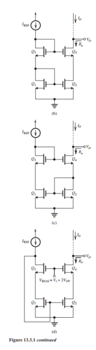
In the current-mirror circuits in Fig. 13.3.1, all transistors are operating at the same current and have the same and the same . Identify each current-mirror (i.e., give its name) and give its output resistance in terms of , and . Also, give the minimum voltage each mirror requires to operate properly. Give in terms of and .
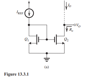
(a) Simple or basic current mirror.
(b) Cascode current mirror.
where
Thus,
(c) Modified Wilson current mirror. is the same as that of the cascode mirror,
Also, is the same as that of the cascode mirror,
(d) Wide-swing current mirror. is the same as that of the cascode,
However, here is
4
Figure 14.1.1
It is required to design a fifth-order Butterworth low-pass filter with a de gain of unity, a passband edge of , and a maximum deviation in the passband transmission of (i.e., ).
(a) Find the transfer function and give and of each of the two pairs of complex-conjugate poles. Also, specify the frequency of the real pole.
(b) Provide a complete circuit realization of the filter as a cascade of two second-order sections and a first-order section. For the second-order sections, use realizations based on the inductancesimulation circuit of Fig. 14.1.1. For the first-order section, use an op amp-RC circuit. Design so that all capacitors are equal to and as many of the resistors as possible are equal. Give the complete circuit and specify the values of all resistors.
(c) What is the attenuation achieved at the stopband edge, ?
Unlock Deck
Unlock for access to all 9 flashcards in this deck.
Unlock Deck
k this deck
5
In the cross-coupled oscillator circuit shown in Fig. 15.1.1, represents the loss of each inductor. Each transistor is operating at a transconductance and has an output resistance . Find the oscillation frequency and explain why the circuit oscillates at this frequency. Also, derive an expression for the minimum value of needed to obtain sustained oscillations.
Figure 15.1.1
Figure 15.1.1
Unlock Deck
Unlock for access to all 9 flashcards in this deck.
Unlock Deck
k this deck
6
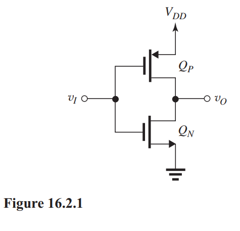
Figure 16.1.1
(a) For the CMOS inverter in Fig. 16.1.1, and have and . Sketch and clearly label the VTC versus and give values for the noise margins and . What is the output resistance when ?
(b) Provide the CMOS realization of the logic function.
Unlock Deck
Unlock for access to all 9 flashcards in this deck.
Unlock Deck
k this deck
7
The CMOS inverter shown in Fig. 16.2.1 has and is fabricated in a process for which , and . For this problem, neglect the Early effect. Both and use the minimum channel length allowed. For .
(a) Find the dimensions that must have in order for the inverter switching to occur at .
(b) What are the noise margins of the inverter?
(c) What current flows in and at the switching point?
(d) For , what is the maximum current that can sink while is limited to ?
Unlock Deck
Unlock for access to all 9 flashcards in this deck.
Unlock Deck
k this deck
8
Figure 16.3.1
The CMOS inverter shown in Fig. 16.3.1 is fabricated in a technology having , , and .
(a) Find to obtain matched transistors.
(b) For , find the maximum load current that the inverter can sink while is not exceeding .
Unlock Deck
Unlock for access to all 9 flashcards in this deck.
Unlock Deck
k this deck
9
Figure 16.4.1
The transistors in the CMOS inverter in Fig. 16.4.1 have , and .
(a) What is the value of the gate threshold?
(b) For , what is the resistance between the output terminal and the supply? If a resistance is connected between the output terminal and ground, what will be?
Unlock Deck
Unlock for access to all 9 flashcards in this deck.
Unlock Deck
k this deck
Unlock Deck
Unlock for access to all 9 flashcards in this deck.


