Deck 4: Building Blocks of Integrated-Circuit Amplifiers
Full screen (f)
Question
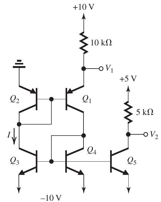
Figure 8.1.1
For the circuit shown in Fig. 8.1.1, assume and are perfectly matched, and , and are perfectly matched. Also, assume all transistors have very high and . Find , and .
Question
Question
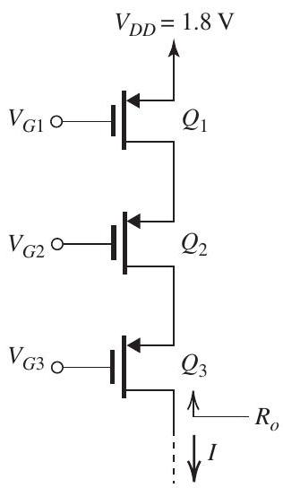
Figure 8.3.1
Design the double-cascode current source shown in Fig. 8.3.1 to provide and the largest possible signal swing at the output; that is, design for the minimum allowable voltage across each transistor. The CMOS fabrication process available has , and . Use devices with , and operate at .
(a) Specify , and .
(b) Find the ratios of the transistors.
(c) What is the value of achieved?
(d) What is the maximum allowable voltage at the current-source output?
(e) If this current source is used as the load of an NMOS double-cascode amplifier having a shortcircuit transconductance of and an output resistance equal to of the current source, what voltage gain is obtained?
Question
Figure 8.4.1
The cascode current source in Fig. 8.4.1 utilizes two identical PMOS transistors fabricated in a 0.18 - CMOS process for which , , and .
Design the circuit to obtain and and to allow for the maximum possible voltage swing at the output terminal of the current source. Utilize . Specify the values of and for and . As well, specify the required values of the dc bias voltages and . What is the maximum allowable voltage at the output?
Question
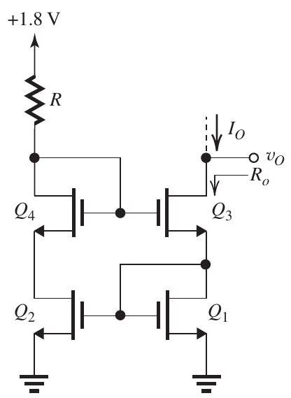
Figure 8.5.1
The modified Wilson current mirror of Fig. 8.5.1 utilizes four matched transistors for which , and . It is required to design the circuit so that with all transistors operating at .
(a) Find the required value of .
(b) Find the required value of the ratio for each of the four transistors.
(c) Find the value of the output resistance .
(d) What is the minimum voltage permitted at the output?

Unlock Deck
Sign up to unlock the cards in this deck!
Unlock Deck
Unlock Deck
1/5
Play
Full screen (f)
Deck 4: Building Blocks of Integrated-Circuit Amplifiers
1
Figure 8.1.1
For the circuit shown in Fig. 8.1.1, assume and are perfectly matched, and , and are perfectly matched. Also, assume all transistors have very high and . Find , and .
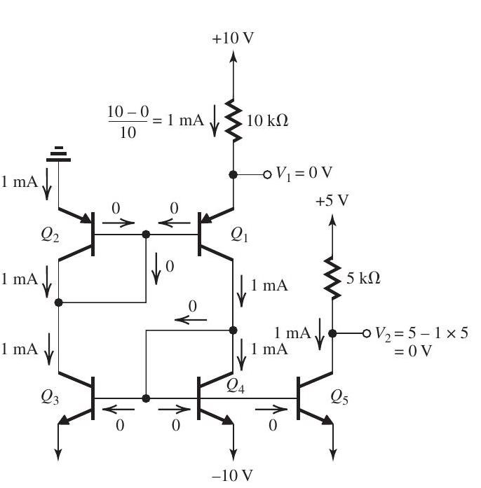
Figure 8.1.2
The analysis is shown on Fig. 8.1.2.
2
Given the availability of NMOS and PMOS transistors that are matched and have and , give circuits for the following amplifiers. In each case, find the output resistance and the voltage gain. In all cases, operate each transistor at a dc bias current of and give the value of at which each transistor is operating.
(a) An NMOS common-source amplifier with a PMOS current-source load.
(b) An NMOS common-source amplifier with an NMOS cascode stage and a single-transistor PMOS current-source load.
(c) An NMOS common-source amplifier with an NMOS cascode stage and a cascode PMOS current-source load.
(a) An NMOS common-source amplifier with a PMOS current-source load.
(b) An NMOS common-source amplifier with an NMOS cascode stage and a single-transistor PMOS current-source load.
(c) An NMOS common-source amplifier with an NMOS cascode stage and a cascode PMOS current-source load.
For each transistor,
(a)
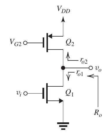
Figure 8.2.1
See Figure 8.2.1.
(b)
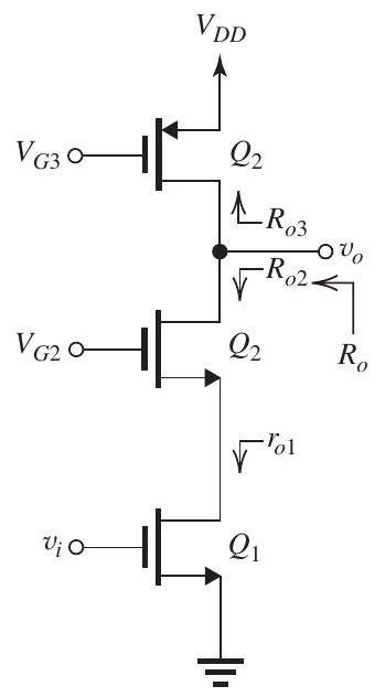
Figure 8.2.2
(c)
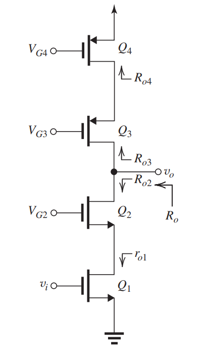
Figure 8.2.3
(a)
Figure 8.2.1
See Figure 8.2.1.
(b)
Figure 8.2.2
(c)
Figure 8.2.3
3
Figure 8.3.1
Design the double-cascode current source shown in Fig. 8.3.1 to provide and the largest possible signal swing at the output; that is, design for the minimum allowable voltage across each transistor. The CMOS fabrication process available has , and . Use devices with , and operate at .
(a) Specify , and .
(b) Find the ratios of the transistors.
(c) What is the value of achieved?
(d) What is the maximum allowable voltage at the current-source output?
(e) If this current source is used as the load of an NMOS double-cascode amplifier having a shortcircuit transconductance of and an output resistance equal to of the current source, what voltage gain is obtained?
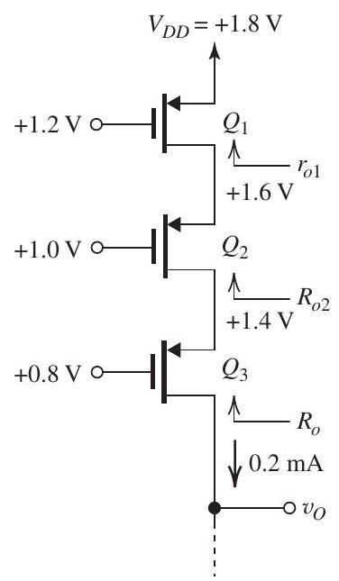
Figure 8.3.2
(a) Refer to Figure 8.3.2. For and and the minimum required for each transistor is . Thus,
and
(b)
(c)
(d)
(e)
4
Figure 8.4.1
The cascode current source in Fig. 8.4.1 utilizes two identical PMOS transistors fabricated in a 0.18 - CMOS process for which , , and .
Design the circuit to obtain and and to allow for the maximum possible voltage swing at the output terminal of the current source. Utilize . Specify the values of and for and . As well, specify the required values of the dc bias voltages and . What is the maximum allowable voltage at the output?
Unlock Deck
Unlock for access to all 5 flashcards in this deck.
Unlock Deck
k this deck
5
Figure 8.5.1
The modified Wilson current mirror of Fig. 8.5.1 utilizes four matched transistors for which , and . It is required to design the circuit so that with all transistors operating at .
(a) Find the required value of .
(b) Find the required value of the ratio for each of the four transistors.
(c) Find the value of the output resistance .
(d) What is the minimum voltage permitted at the output?
Unlock Deck
Unlock for access to all 5 flashcards in this deck.
Unlock Deck
k this deck
Unlock Deck
Unlock for access to all 5 flashcards in this deck.


