Deck 7: BJT Power Amplifiers
Full screen (f)
Question
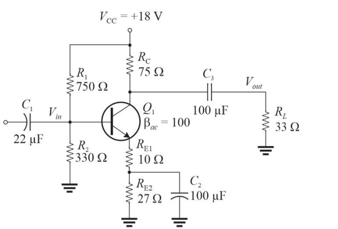 Figure 1
Refer to Figure 1. The voltage gain, Av, to the load is approximately
A)11
B)7.5
C)5.4
D)2.0
Question
Question
Question
Question
 Figure 7
Refer to Figure 7. The expected dc emitter voltage for Q1 is
A)0 V
B)9.0 V
C)0.7 V
D)8.3 V
Question
Question
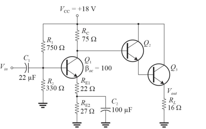 Figure 2 This is modification of Figure 1 (added Q2, Q3, and RL, deletion of C3 and a changed value of RE1).
Refer to Figure 2. With no applied signal, the dc power dissipated in the load is approximately
A)1.1 W
B)0
C)5.5 W
D)2.8 W
Question
 Figure 3
Refer to Figure 3. Note the input is a 5 Vrms sine wave. The ac power in RL is ideally
A)1.56 W
B)3.12 W
C)0.31 W
D)0.62 W
Question
Question
Figure 2 This is modification of Figure 1 (added Q2, Q3, and RL, deletion of C3 and a changed value of RE1).Refer to Figure 2. If Vin = 1 Vrms, the ac power in RL is approximately
A)2.6 W
B)4.0 W
C)680 mW
D)1.3 W
Question
 Figure 1
Refer to Figure 1. The input impedance is approximately
A)230 ▲
B)186 ▲
C)125 ▲
D)142 ▲
Question
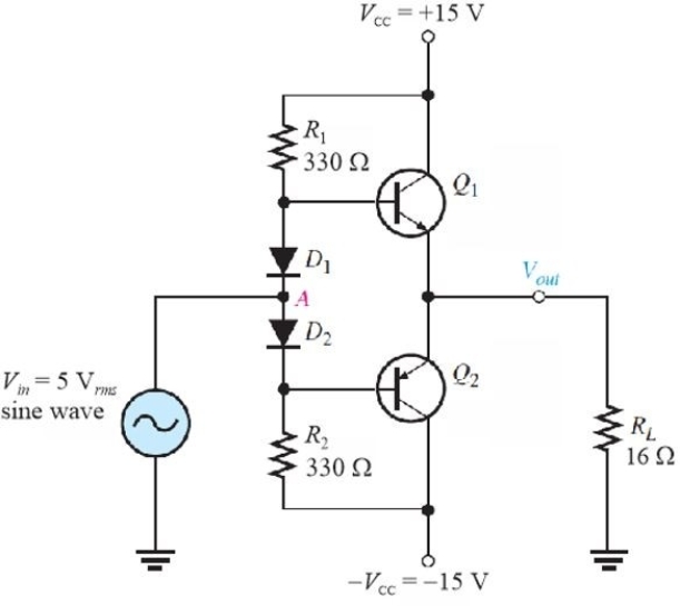 Figure 3
Refer to Figure 3. The value of dc bias current in R1 is
A)43 mA
B)90 mA
C)86 mA
D)48 mA
Question
 Figure 3
Refer to Figure 3. With no signal in, IC(Q1)is ideally
A)0
B)86 mA
C)43 mA
D)48 mA
Question
Question
 Figure 5
Refer to Figure 5. The diode
A)produces class- AB operation
B)compensates for the base- emitter drops of the transistors
C)helps prevent crossover distortion
D)all of the above
Question
 Figure 7
Refer to Figure 7. The power delivered to the load is
A)0.25 W
B)1 W
C)0.5 W
D)2 W
Question
 Figure 1
Refer to Figure 1. The power gain, Ap, to the load is approximately
A)14
B)4.5
C)23
D)7.9
Question
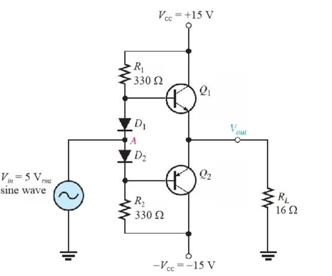 Figure 3
Refer to Figure 3. This type of bias is called
A)current- mirror biasing
B)push- pull bias
C)diode biasing
D)mid- point bias
Question
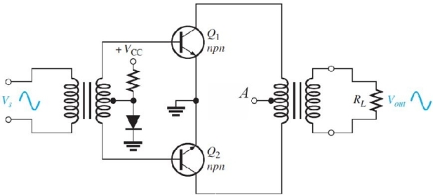 Figure 5
Refer to Figure 5. The center tap on the output transformer (marked
A)should be connected to
A)-VCC
B)ground
C)+VCC D)nothing, it is left open
Question
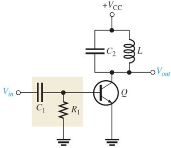 Figure 6
Refer to Figure 6. The combination of R1, C1, and the base- emitter diode form a
A)positive clipping circuit
B)clamping circuit
C)negative clipping circuit
D)coupling circuit
Question
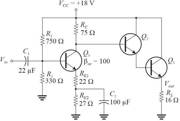 Figure 2 This is modification of Figure 1 (added Q2, Q3, and RL, deletion of C3 and a changed value of RE1).
Refer to Figure 2. Assume Vout has dropped to about 1/2 the expected value. A likely cause is that
A)VCC is set to +15 V
B)C2 is shorted
C)RL is open
D)C2 is open
Question
Question
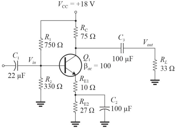 Figure 1
Refer to Figure 1. The dc collector current is approximately
A)50 mA
B)25 mA
C)120 mA
D)85 mA
Question
Question
Question
Question
Question
Question
 Figure 6
The transistor in a Class- C amplifier is biased for conduction for
A)360°
B)90°
C)180°
D)much less than 90°
Question
Question
Question
 Figure 4
Refer to Figure 4. The amplifier represented is
A)class- C
B)class- A
C)class- B
Question
Question
 Figure 7
Refer to Figure 7. The expected ac emitter voltage for Q1 is
A)4.0 Vrms
B)2.0 Vrms
C)0 V
D)none of the above
Question
 Figure 2 This is modification of Figure 1 (added Q2, Q3, and RL, deletion of C3 and a changed value of RE1).
Refer to Figure 2, which is a modified circuit from Figure 1. The voltage gain, AV, of this circuit is approximately
A)3.3
B)5.6
C)2.0
D)4.3

Unlock Deck
Sign up to unlock the cards in this deck!
Unlock Deck
Unlock Deck
1/35
Play
Full screen (f)
Deck 7: BJT Power Amplifiers
1
Figure 1Refer to Figure 1. The voltage gain, Av, to the load is approximately
A)11
B)7.5
C)5.4
D)2.0
D
2
The amplifier type that frequently has a resonant circuit load is
A)class- AB
B)class- C
C)class- B
D)class- A
A)class- AB
B)class- C
C)class- B
D)class- A
B
3
The amplifier type that has the worst efficiency is
A)class- B
B)class- A
C)class- C
D)class- AB
A)class- B
B)class- A
C)class- C
D)class- AB
B
4
In a single- stage class- A amplifier, the quiescent current is the same as the
A)ac load current
B)dc collector current
C)ac collector current
D)bias current
A)ac load current
B)dc collector current
C)ac collector current
D)bias current
Unlock Deck
Unlock for access to all 35 flashcards in this deck.
Unlock Deck
k this deck
5
Figure 7Refer to Figure 7. The expected dc emitter voltage for Q1 is
A)0 V
B)9.0 V
C)0.7 V
D)8.3 V
Unlock Deck
Unlock for access to all 35 flashcards in this deck.
Unlock Deck
k this deck
6
A heat sink is used to
A)prevent excessive current
B)reduce the junction temperature
C)reduce ambient temperature
D)all of the above
A)prevent excessive current
B)reduce the junction temperature
C)reduce ambient temperature
D)all of the above
Unlock Deck
Unlock for access to all 35 flashcards in this deck.
Unlock Deck
k this deck
7
Figure 2 This is modification of Figure 1 (added Q2, Q3, and RL, deletion of C3 and a changed value of RE1).Refer to Figure 2. With no applied signal, the dc power dissipated in the load is approximately
A)1.1 W
B)0
C)5.5 W
D)2.8 W
Unlock Deck
Unlock for access to all 35 flashcards in this deck.
Unlock Deck
k this deck
8
Figure 3Refer to Figure 3. Note the input is a 5 Vrms sine wave. The ac power in RL is ideally
A)1.56 W
B)3.12 W
C)0.31 W
D)0.62 W
Unlock Deck
Unlock for access to all 35 flashcards in this deck.
Unlock Deck
k this deck
9
A class- A amplifier has an input resistance of 520 ▲ and a load resistance of 26 ▲. Assume a 1 Vrms input produces a 5 Vrms output The power gain is
A)5
B)100
C)50
D)500
A)5
B)100
C)50
D)500
Unlock Deck
Unlock for access to all 35 flashcards in this deck.
Unlock Deck
k this deck
10
Figure 2 This is modification of Figure 1 (added Q2, Q3, and RL, deletion of C3 and a changed value of RE1).Refer to Figure 2. If Vin = 1 Vrms, the ac power in RL is approximately
A)2.6 W
B)4.0 W
C)680 mW
D)1.3 W
Unlock Deck
Unlock for access to all 35 flashcards in this deck.
Unlock Deck
k this deck
11
Figure 1Refer to Figure 1. The input impedance is approximately
A)230 ▲
B)186 ▲
C)125 ▲
D)142 ▲
Unlock Deck
Unlock for access to all 35 flashcards in this deck.
Unlock Deck
k this deck
12
Figure 3Refer to Figure 3. The value of dc bias current in R1 is
A)43 mA
B)90 mA
C)86 mA
D)48 mA
Unlock Deck
Unlock for access to all 35 flashcards in this deck.
Unlock Deck
k this deck
13
Figure 3Refer to Figure 3. With no signal in, IC(Q1)is ideally
A)0
B)86 mA
C)43 mA
D)48 mA
Unlock Deck
Unlock for access to all 35 flashcards in this deck.
Unlock Deck
k this deck
14
Assume the Q point on a class- A amplifier is centered on the ac load line. The maximum peak- to- peak output voltage is
A)1/2 VCEQ
B)2 VCEQ
C)1/2 VCC
D)VCEQ
A)1/2 VCEQ
B)2 VCEQ
C)1/2 VCC
D)VCEQ
Unlock Deck
Unlock for access to all 35 flashcards in this deck.
Unlock Deck
k this deck
15
Figure 5Refer to Figure 5. The diode
A)produces class- AB operation
B)compensates for the base- emitter drops of the transistors
C)helps prevent crossover distortion
D)all of the above
Unlock Deck
Unlock for access to all 35 flashcards in this deck.
Unlock Deck
k this deck
16
Figure 7Refer to Figure 7. The power delivered to the load is
A)0.25 W
B)1 W
C)0.5 W
D)2 W
Unlock Deck
Unlock for access to all 35 flashcards in this deck.
Unlock Deck
k this deck
17
Figure 1Refer to Figure 1. The power gain, Ap, to the load is approximately
A)14
B)4.5
C)23
D)7.9
Unlock Deck
Unlock for access to all 35 flashcards in this deck.
Unlock Deck
k this deck
18
Figure 3Refer to Figure 3. This type of bias is called
A)current- mirror biasing
B)push- pull bias
C)diode biasing
D)mid- point bias
Unlock Deck
Unlock for access to all 35 flashcards in this deck.
Unlock Deck
k this deck
19
Figure 5Refer to Figure 5. The center tap on the output transformer (marked
A)should be connected to
A)-VCC
B)ground
C)+VCC D)nothing, it is left open
Unlock Deck
Unlock for access to all 35 flashcards in this deck.
Unlock Deck
k this deck
20
Figure 6Refer to Figure 6. The combination of R1, C1, and the base- emitter diode form a
A)positive clipping circuit
B)clamping circuit
C)negative clipping circuit
D)coupling circuit
Unlock Deck
Unlock for access to all 35 flashcards in this deck.
Unlock Deck
k this deck
21
Figure 2 This is modification of Figure 1 (added Q2, Q3, and RL, deletion of C3 and a changed value of RE1).Refer to Figure 2. Assume Vout has dropped to about 1/2 the expected value. A likely cause is that
A)VCC is set to +15 V
B)C2 is shorted
C)RL is open
D)C2 is open
Unlock Deck
Unlock for access to all 35 flashcards in this deck.
Unlock Deck
k this deck
22
Class- C amplifiers are frequently used as audio amplifiers.
Unlock Deck
Unlock for access to all 35 flashcards in this deck.
Unlock Deck
k this deck
23
Figure 1Refer to Figure 1. The dc collector current is approximately
A)50 mA
B)25 mA
C)120 mA
D)85 mA
Unlock Deck
Unlock for access to all 35 flashcards in this deck.
Unlock Deck
k this deck
24
A class- B amplifier with Darlington transistors can use larger bias resistors.
Unlock Deck
Unlock for access to all 35 flashcards in this deck.
Unlock Deck
k this deck
25
The ratio of Pout to PDC is the efficiency of an amplifier.
Unlock Deck
Unlock for access to all 35 flashcards in this deck.
Unlock Deck
k this deck
26
The Q point of a class- C amplifier is below cutoff.
Unlock Deck
Unlock for access to all 35 flashcards in this deck.
Unlock Deck
k this deck
27
The maximum power from a class- A amplifier is equal to ICQVCEQ.
Unlock Deck
Unlock for access to all 35 flashcards in this deck.
Unlock Deck
k this deck
28
In a class- AB amplifier, the transistors are biased slightly above cutoff to avoid
A)clipping the peaks of signals
B)low efficiency
C)loading problems
D)crossover distortion
A)clipping the peaks of signals
B)low efficiency
C)loading problems
D)crossover distortion
Unlock Deck
Unlock for access to all 35 flashcards in this deck.
Unlock Deck
k this deck
29
Figure 6The transistor in a Class- C amplifier is biased for conduction for
A)360°
B)90°
C)180°
D)much less than 90°
Unlock Deck
Unlock for access to all 35 flashcards in this deck.
Unlock Deck
k this deck
30
In a class- B amplifier, the Q- point is at cutoff.
Unlock Deck
Unlock for access to all 35 flashcards in this deck.
Unlock Deck
k this deck
31
The maximum ideal efficiency for a class- A amplifier is
A)80%
B)40%
C)55%
D)25%
A)80%
B)40%
C)55%
D)25%
Unlock Deck
Unlock for access to all 35 flashcards in this deck.
Unlock Deck
k this deck
32
Figure 4Refer to Figure 4. The amplifier represented is
A)class- C
B)class- A
C)class- B
Unlock Deck
Unlock for access to all 35 flashcards in this deck.
Unlock Deck
k this deck
33
A class- A amplifier the quiescent power is dissipated only when a signal is present.
Unlock Deck
Unlock for access to all 35 flashcards in this deck.
Unlock Deck
k this deck
34
Figure 7Refer to Figure 7. The expected ac emitter voltage for Q1 is
A)4.0 Vrms
B)2.0 Vrms
C)0 V
D)none of the above
Unlock Deck
Unlock for access to all 35 flashcards in this deck.
Unlock Deck
k this deck
35
Figure 2 This is modification of Figure 1 (added Q2, Q3, and RL, deletion of C3 and a changed value of RE1).Refer to Figure 2, which is a modified circuit from Figure 1. The voltage gain, AV, of this circuit is approximately
A)3.3
B)5.6
C)2.0
D)4.3
Unlock Deck
Unlock for access to all 35 flashcards in this deck.
Unlock Deck
k this deck
Unlock Deck
Unlock for access to all 35 flashcards in this deck.


