Deck 8: Field-Effect Transistors Fets
Full screen (f)
Question
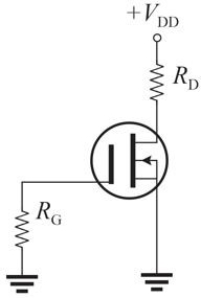 Figure 4
Refer to Figure 4. The transistor is biased for
A)depletion mode
B)enhancement mode
C)neither
Question
Question
 Figure 1
Refer to Figure 1, which represents two curves for a JFET. At ID = 6 mA, the transconductance, gm, is approximately
A)7700 µmho
B)3400 µmho
C)4300 µmho
D)12,000 µmho
Question
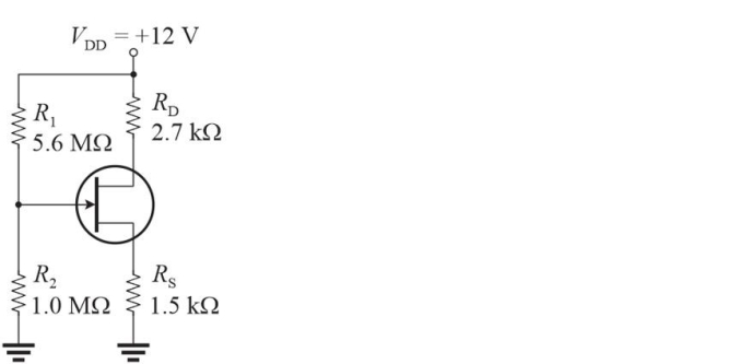 Figure 3 Assume IDSS = 3.5 mA and VGS(off)= -2 V.
Refer to Figure 3. An advantage to the voltage divider bias over self- bias is that voltage- divider bias
A)allows for greater variation in JFET parameters
B)has higher input resistance
C)enables the gate- source to be forward- biased or reverse- biased
D)all of the above
Question
 Figure 3 Assume IDSS = 3.5 mA and VGS(off)= -2 V.
If a JFET bias circuit is designed with current- source biasing,
A)ID is constant for any JFET
B)IDSS is constant for any JFET
C)VGS is constant for any JFET
D)VGS(off)is constant for any JFET
Question
 Figure 1
Refer to Figure 1. The source resistor, RS, that would self- bias this JFET at approximately VGS = -2 V is
A)220 ▲
B)470 ▲
C)360 ▲
D)1 M▲
Question
 Figure 2 Assume the curve in (b)represents the transistor in (a).
Refer to Figure 2. If VS = 1.3 V, then VGS is
A)0 V
B)1.3 V
C)-1.3 V
D)4.0 V
Question
 Figure 1
Refer to Figure 1. The curve on the left is called the
A)negative resistance curve
B)transconductance curve
C)transfer curve
D)characteristic curve
Question
Question
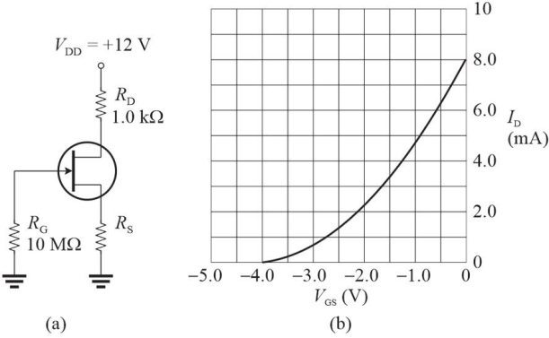 Figure 2 Assume the curve in (b)represents the transistor in (a).
Refer to Figure 2. IDSS is approximately
A)4.0 mA
B)6.0 mA
C)3.3 mA
D)8.0 mA
Question
Question
 Figure 5 The equations for K and ID are given in part (c).
Refer to Figure 5. ID is approximately
A)2.2 mA
B)0.88 mA
C)3.4 mA
D)1.2 mA
Question
Question
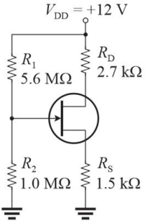 Figure 3 Assume IDSS = 3.5 mA and VGS(off)= -2 V.
Refer to Figure 3. If the drain voltage, VD, is 7.6 V, what is VGS?
A)-0.62 V
B)-1.8 V
C)-1.5 V
D)-4.2 V
Question
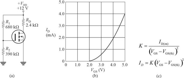 Figure 5 The equations for K and ID are given in part (c).
Refer to Figure 5. VGS is
A)6.9 V
B)4.4 V
C)7.6 V
D)3.6 V
Question
Question
 Figure 3 Assume IDSS = 3.5 mA and VGS(off)= -2 V.
Refer to Figure 3. If RS were shorted to ground, the current, ID, is
A)1/2 IDSS
B)0 mA
C)> IDSS
D)IDSS
Question
 Figure 1
Refer to Figure 1. The pinch- off voltage, Vp, is
A)-2.5 V
B)+5 V
C)-5 V
D)0 V
Question
Question
Question
Question
Figure 5 The equations for K and ID are given in part (c).Refer to Figure 5. The transistor shown is a
A)p- channel E- MOSFET
B)p- channel D- MOSFET
C)n- channel D- MOSFET
D)n- channel E- MOSFET
Question
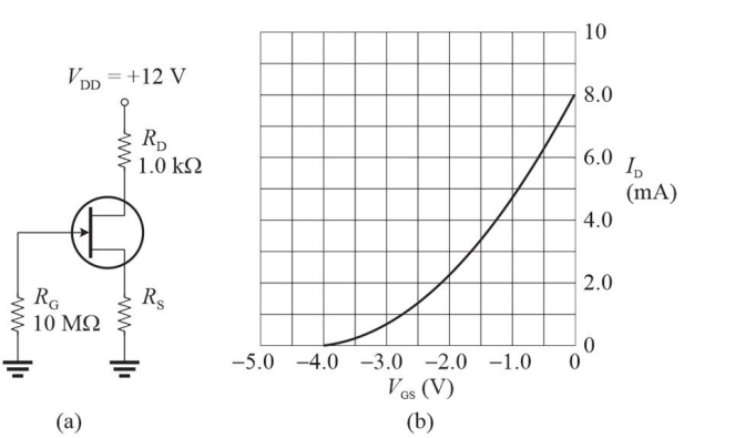 Figure 2 Assume the curve in (b)represents the transistor in (a).
Refer to Figure 2. A source resistor, RS, that will provide approximately ID = 4 mA is
A)250 W
B)560 ▲
C)470 ▲
D)330 ▲
Question
Question
Question
Question
Question
Question
Question
Question
Question
 Figure 2 Assume the curve in (b)represents the transistor in (a).
Refer to Figure 2. Assume that the source terminal is grounded. For this transistor, the drain voltage, VD, will be approximately
A)4.0 V
B)0 V
C)12 V
D)8.0 V
Question

Unlock Deck
Sign up to unlock the cards in this deck!
Unlock Deck
Unlock Deck
1/33
Play
Full screen (f)
Deck 8: Field-Effect Transistors Fets
1
Figure 4Refer to Figure 4. The transistor is biased for
A)depletion mode
B)enhancement mode
C)neither
C
2
A certain MOSFET has IDSS = 6 mA, VGS = -0.67 V, and VGS(off )= -5 V. The drain current, ID is
A)3.0 mA
B)0.75 mA
C)1.5 mA
D)4.5 Ma
A)3.0 mA
B)0.75 mA
C)1.5 mA
D)4.5 Ma
D
3
Figure 1Refer to Figure 1, which represents two curves for a JFET. At ID = 6 mA, the transconductance, gm, is approximately
A)7700 µmho
B)3400 µmho
C)4300 µmho
D)12,000 µmho
B
4
Figure 3 Assume IDSS = 3.5 mA and VGS(off)= -2 V.Refer to Figure 3. An advantage to the voltage divider bias over self- bias is that voltage- divider bias
A)allows for greater variation in JFET parameters
B)has higher input resistance
C)enables the gate- source to be forward- biased or reverse- biased
D)all of the above
Unlock Deck
Unlock for access to all 33 flashcards in this deck.
Unlock Deck
k this deck
5
Figure 3 Assume IDSS = 3.5 mA and VGS(off)= -2 V.If a JFET bias circuit is designed with current- source biasing,
A)ID is constant for any JFET
B)IDSS is constant for any JFET
C)VGS is constant for any JFET
D)VGS(off)is constant for any JFET
Unlock Deck
Unlock for access to all 33 flashcards in this deck.
Unlock Deck
k this deck
6
Figure 1Refer to Figure 1. The source resistor, RS, that would self- bias this JFET at approximately VGS = -2 V is
A)220 ▲
B)470 ▲
C)360 ▲
D)1 M▲
Unlock Deck
Unlock for access to all 33 flashcards in this deck.
Unlock Deck
k this deck
7
Figure 2 Assume the curve in (b)represents the transistor in (a).Refer to Figure 2. If VS = 1.3 V, then VGS is
A)0 V
B)1.3 V
C)-1.3 V
D)4.0 V
Unlock Deck
Unlock for access to all 33 flashcards in this deck.
Unlock Deck
k this deck
8
Figure 1Refer to Figure 1. The curve on the left is called the
A)negative resistance curve
B)transconductance curve
C)transfer curve
D)characteristic curve
Unlock Deck
Unlock for access to all 33 flashcards in this deck.
Unlock Deck
k this deck
9
An advantage of a JFET over a BJT is that the JFET has
A)higher input resistance
B)higher gain
C)better linearity
D)all of the above
A)higher input resistance
B)higher gain
C)better linearity
D)all of the above
Unlock Deck
Unlock for access to all 33 flashcards in this deck.
Unlock Deck
k this deck
10
Figure 2 Assume the curve in (b)represents the transistor in (a).Refer to Figure 2. IDSS is approximately
A)4.0 mA
B)6.0 mA
C)3.3 mA
D)8.0 mA
Unlock Deck
Unlock for access to all 33 flashcards in this deck.
Unlock Deck
k this deck
11
The IGBT has characteristics of a
A)JFET input and BJT output
B)MOSFET input and a BJT output
C)BJT input and a JFET output
D)none of the above
A)JFET input and BJT output
B)MOSFET input and a BJT output
C)BJT input and a JFET output
D)none of the above
Unlock Deck
Unlock for access to all 33 flashcards in this deck.
Unlock Deck
k this deck
12
Figure 5 The equations for K and ID are given in part (c).Refer to Figure 5. ID is approximately
A)2.2 mA
B)0.88 mA
C)3.4 mA
D)1.2 mA
Unlock Deck
Unlock for access to all 33 flashcards in this deck.
Unlock Deck
k this deck
13
Assume a transistor has an IDSS of 3.0 mA and a gm0 of 2500 µS. The gate- source cutoff voltage, VGS(off), is
A)-1.2 V
B)-1.8 V
C)-0.6 V
D)-2.4 V
A)-1.2 V
B)-1.8 V
C)-0.6 V
D)-2.4 V
Unlock Deck
Unlock for access to all 33 flashcards in this deck.
Unlock Deck
k this deck
14
Figure 3 Assume IDSS = 3.5 mA and VGS(off)= -2 V.Refer to Figure 3. If the drain voltage, VD, is 7.6 V, what is VGS?
A)-0.62 V
B)-1.8 V
C)-1.5 V
D)-4.2 V
Unlock Deck
Unlock for access to all 33 flashcards in this deck.
Unlock Deck
k this deck
15
Figure 5 The equations for K and ID are given in part (c).Refer to Figure 5. VGS is
A)6.9 V
B)4.4 V
C)7.6 V
D)3.6 V
Unlock Deck
Unlock for access to all 33 flashcards in this deck.
Unlock Deck
k this deck
16
A FET that has no channel until one is induced electrically is
A)an E- MOSFET
B)a VMOSFET
C)a p- channel JFET
D)a D- MOSFET
A)an E- MOSFET
B)a VMOSFET
C)a p- channel JFET
D)a D- MOSFET
Unlock Deck
Unlock for access to all 33 flashcards in this deck.
Unlock Deck
k this deck
17
Figure 3 Assume IDSS = 3.5 mA and VGS(off)= -2 V.Refer to Figure 3. If RS were shorted to ground, the current, ID, is
A)1/2 IDSS
B)0 mA
C)> IDSS
D)IDSS
Unlock Deck
Unlock for access to all 33 flashcards in this deck.
Unlock Deck
k this deck
18
Figure 1Refer to Figure 1. The pinch- off voltage, Vp, is
A)-2.5 V
B)+5 V
C)-5 V
D)0 V
Unlock Deck
Unlock for access to all 33 flashcards in this deck.
Unlock Deck
k this deck
19
A JFET that is operating as a voltage- controlled resistance is
A)typically biased near the origin
B)has minimum resistance at VGS = 0
C)is operating in the ohmic region
D)all of the above
A)typically biased near the origin
B)has minimum resistance at VGS = 0
C)is operating in the ohmic region
D)all of the above
Unlock Deck
Unlock for access to all 33 flashcards in this deck.
Unlock Deck
k this deck
20
An E- MOSFET cannot use
A)drain- feedback bias
B)voltage- divider bias
C)self- bias
A)drain- feedback bias
B)voltage- divider bias
C)self- bias
Unlock Deck
Unlock for access to all 33 flashcards in this deck.
Unlock Deck
k this deck
21
The transconductance curve has the same shape as the transfer curve.
Unlock Deck
Unlock for access to all 33 flashcards in this deck.
Unlock Deck
k this deck
22
Figure 5 The equations for K and ID are given in part (c).Refer to Figure 5. The transistor shown is a
A)p- channel E- MOSFET
B)p- channel D- MOSFET
C)n- channel D- MOSFET
D)n- channel E- MOSFET
Unlock Deck
Unlock for access to all 33 flashcards in this deck.
Unlock Deck
k this deck
23
Figure 2 Assume the curve in (b)represents the transistor in (a).Refer to Figure 2. A source resistor, RS, that will provide approximately ID = 4 mA is
A)250 W
B)560 ▲
C)470 ▲
D)330 ▲
Unlock Deck
Unlock for access to all 33 flashcards in this deck.
Unlock Deck
k this deck
24
JFETs and MOSFETs are often referred to as square- law devices.
Unlock Deck
Unlock for access to all 33 flashcards in this deck.
Unlock Deck
k this deck
25
The maximum drain current in a JFET is IDSS, which occurs at VGS = 0 V.
Unlock Deck
Unlock for access to all 33 flashcards in this deck.
Unlock Deck
k this deck
26
Dual- gate MOSFETs can be either depletion or enhancement devices.
Unlock Deck
Unlock for access to all 33 flashcards in this deck.
Unlock Deck
k this deck
27
All MOSFETs are subject to damage from electrostatic discharge.
Unlock Deck
Unlock for access to all 33 flashcards in this deck.
Unlock Deck
k this deck
28
An n- channel E- MOSFET
A)can use either a positive or a negative gate voltage to conduct
B)requires a negative gate voltage to conduct
C)can have an open gate and still conduct
D)requires a positive gate voltage to conduct
A)can use either a positive or a negative gate voltage to conduct
B)requires a negative gate voltage to conduct
C)can have an open gate and still conduct
D)requires a positive gate voltage to conduct
Unlock Deck
Unlock for access to all 33 flashcards in this deck.
Unlock Deck
k this deck
29
The most important application for an IGBT is in
A)high frequency amplifiers
B)logic circuits
C)high voltage and high current switching
D)power linear amplifiers
A)high frequency amplifiers
B)logic circuits
C)high voltage and high current switching
D)power linear amplifiers
Unlock Deck
Unlock for access to all 33 flashcards in this deck.
Unlock Deck
k this deck
30
For normal operation, the gate- source junction of a JFET is reverse- biased.
Unlock Deck
Unlock for access to all 33 flashcards in this deck.
Unlock Deck
k this deck
31
The input structure of a MOSFET is a reverse- biased diode.
Unlock Deck
Unlock for access to all 33 flashcards in this deck.
Unlock Deck
k this deck
32
Figure 2 Assume the curve in (b)represents the transistor in (a).Refer to Figure 2. Assume that the source terminal is grounded. For this transistor, the drain voltage, VD, will be approximately
A)4.0 V
B)0 V
C)12 V
D)8.0 V
Unlock Deck
Unlock for access to all 33 flashcards in this deck.
Unlock Deck
k this deck
33
Assume an n- channel JFET has a VGS(off)of -8 V. If VGS = -4 V, ID will be
A)IDSS
B)1/4 IDSS
C)1/2 IDSS
D)3/4 IDSS
A)IDSS
B)1/4 IDSS
C)1/2 IDSS
D)3/4 IDSS
Unlock Deck
Unlock for access to all 33 flashcards in this deck.
Unlock Deck
k this deck
Unlock Deck
Unlock for access to all 33 flashcards in this deck.


