Deck 16: Oscillators
Full screen (f)
Question
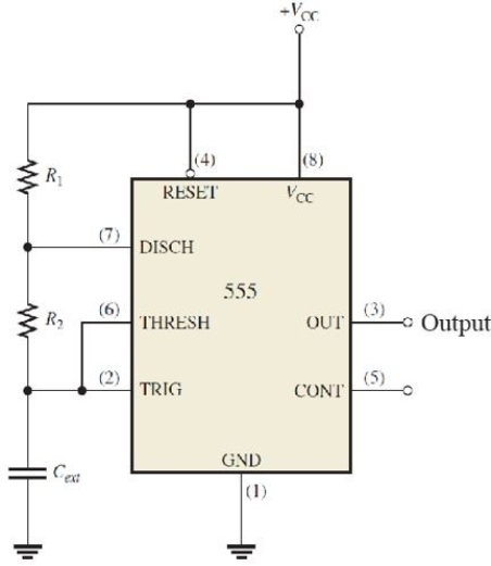 Figure 6
Refer to Figure 6. If a capacitor is place from CONT to ground it will
A)change the output frequency
B)change the output duty cycle
C)both A and B
D)none of the above
Question
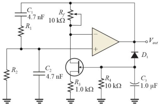 Figure 1
Refer to Figure 1. Assume the frequency of Vout is 6.0 kHz and R1 = R2. The value of each of these resistors is
A)3.6 k▲
B)5.6 k▲
C)27 k▲
D)8.9 k▲
Question
 Figure 6
Refer to Figure 6. The output is a
A)pulses with a duty cycle >50%
B)square wave (duty cycle = 50%)
C)pulses with a duty cycle <50%
D)tringle wave
Question
Figure 1Refer to Figure 1. The JFET acts as a
A)signal reference
B)voltage- controlled current source
C)inverting amplifier
D)voltage- controlled resistor
Question
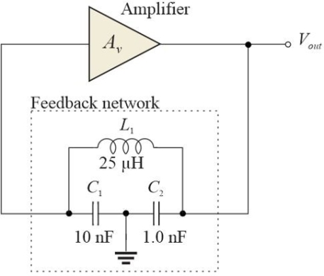 Figure 3 A simplified oscillator circuit.
Refer to Figure 3. The type of oscillator represented is a
A)Hartley
B)Armstrong
C)Clapp
D)Colpitts
Question
 Figure 1
Refer to Figure 5. The output of this circuit is a
A)square wave
B)sine wave
C)sawtooth wave
D)triangle wave
Question
 Figure 6
Refer to Figure 6. The capacitor voltage is between
A)1/3 VCC and 2/3 VCC
B)0 V and 2/3 VCC
C)1/3 VCC and VCC
D)0 V and VCC
Question
Question
Question
 Figure 3 A simplified oscillator circuit.
Refer to Figure 3. Assume the circuit is working normally; the output frequency is approximately
A)100 kHz
B)333 kHz
C)3.33 MHz
D)1.0 MHz
Question
 Figure 2
Refer to Figure 2. The portion in the dashed box is
A)a phase shift network
B)a notch filter
C)a lead- lag network
D)none of the above
Question
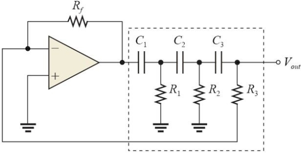 Figure 2
Refer to Figure 2. Rf determines the
A)gain
B)output frequency
C)both A and B
D)none of the above
Question
Question
Figure 1Refer to Figure 1. When adjusted properly the signal at the non- inverting input of the op- amp is
A)2/3 Vout
B)1/3 Vout
C)1/2 Vout
D)none of the above
Question
 Figure 2
Refer to Figure 2. The circuit is
A)a Colpitts oscillator
B)a twin- T oscillator
C)a Wien bridge oscillator
D)none of the above
Question
 Figure 6
Refer to Figure 6. The circuit can be configured as a VCO by applying
A)disconnecting the THRESH and applying a variable voltage to it
B)a variable voltage to the CONT pin
C)disconnecting the RESET and applying a variable voltage to it
D)none of the above
Question
Figure 1Refer to Figure 1. The output of the circuit when adjusted properly is a
A)square wave
B)sinusoidal wave
C)swept frequency
D)triangle wave
Question
 Figure 3 A simplified oscillator circuit.
Refer to Figure 5. This is an example of a
A)function generator
B)voltage- controlled oscillator
C)twin- T oscillator
D)relaxation oscillator
Question
 Figure 3 A simplified oscillator circuit.
Refer to Figure 3. If the inductor is changed for one twice as large, the resonant frequency will be
A)doubled
B)unchanged
C)halved
D)none of the above
Question
Figure 3 A simplified oscillator circuit.Refer to Figure 3. The fraction of the output that is fed back is
A)0.50
B)0.20
C)0.90
D)0.10
Question
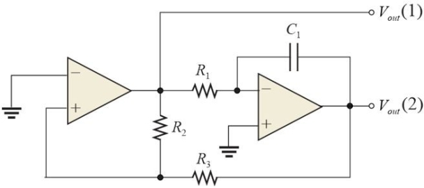 Figure 4
Refer to Figure 4. The output frequency is determined by C1 and
A)R1 and R3
B)R1 and R2
C)R2 and R3
D)R1, R2, and R3
Question
Question
Question
 Figure 2
Refer to Figure 2. The op- amp serves to
A)amplify the feedback signal
B)shift the phase of the feedback signal by 90°
C)both A and B
D)none of the above
Question
Question
Question
Question
Question
Question
Figure 4Refer to Figure 4. The two outputs are a
A)square wave and a triangle wave
B)square wave and a sine wave
C)sawtooth wave and a triangle wave
D)sawtooth wave and a sine wave
Question
Question
Question

Unlock Deck
Sign up to unlock the cards in this deck!
Unlock Deck
Unlock Deck
1/33
Play
Full screen (f)
Deck 16: Oscillators
1
Figure 6Refer to Figure 6. If a capacitor is place from CONT to ground it will
A)change the output frequency
B)change the output duty cycle
C)both A and B
D)none of the above
D
2
Figure 1Refer to Figure 1. Assume the frequency of Vout is 6.0 kHz and R1 = R2. The value of each of these resistors is
A)3.6 k▲
B)5.6 k▲
C)27 k▲
D)8.9 k▲
B
3
Figure 6Refer to Figure 6. The output is a
A)pulses with a duty cycle >50%
B)square wave (duty cycle = 50%)
C)pulses with a duty cycle <50%
D)tringle wave
A
4
Figure 1Refer to Figure 1. The JFET acts as a
A)signal reference
B)voltage- controlled current source
C)inverting amplifier
D)voltage- controlled resistor
Unlock Deck
Unlock for access to all 33 flashcards in this deck.
Unlock Deck
k this deck
5
Figure 3 A simplified oscillator circuit.Refer to Figure 3. The type of oscillator represented is a
A)Hartley
B)Armstrong
C)Clapp
D)Colpitts
Unlock Deck
Unlock for access to all 33 flashcards in this deck.
Unlock Deck
k this deck
6
Figure 1Refer to Figure 5. The output of this circuit is a
A)square wave
B)sine wave
C)sawtooth wave
D)triangle wave
Unlock Deck
Unlock for access to all 33 flashcards in this deck.
Unlock Deck
k this deck
7
Figure 6Refer to Figure 6. The capacitor voltage is between
A)1/3 VCC and 2/3 VCC
B)0 V and 2/3 VCC
C)1/3 VCC and VCC
D)0 V and VCC
Unlock Deck
Unlock for access to all 33 flashcards in this deck.
Unlock Deck
k this deck
8
Closed- loop gain for a feedback oscillator is expressed as
A)Av/B
B)AvB + 1
C)1/B
D)AvB
A)Av/B
B)AvB + 1
C)1/B
D)AvB
Unlock Deck
Unlock for access to all 33 flashcards in this deck.
Unlock Deck
k this deck
9
At startup, a feedback oscillator requires a closed- loop gain of
A)exactly +1
B)exactly -1
C)0
D)none of the above
A)exactly +1
B)exactly -1
C)0
D)none of the above
Unlock Deck
Unlock for access to all 33 flashcards in this deck.
Unlock Deck
k this deck
10
Figure 3 A simplified oscillator circuit.Refer to Figure 3. Assume the circuit is working normally; the output frequency is approximately
A)100 kHz
B)333 kHz
C)3.33 MHz
D)1.0 MHz
Unlock Deck
Unlock for access to all 33 flashcards in this deck.
Unlock Deck
k this deck
11
Figure 2Refer to Figure 2. The portion in the dashed box is
A)a phase shift network
B)a notch filter
C)a lead- lag network
D)none of the above
Unlock Deck
Unlock for access to all 33 flashcards in this deck.
Unlock Deck
k this deck
12
Figure 2Refer to Figure 2. Rf determines the
A)gain
B)output frequency
C)both A and B
D)none of the above
Unlock Deck
Unlock for access to all 33 flashcards in this deck.
Unlock Deck
k this deck
13
The overall response of a twin- T feedback network is that of a
A)parallel resonant circuit
B)bandpass filter
C)lead- lag network
D)notch filter
A)parallel resonant circuit
B)bandpass filter
C)lead- lag network
D)notch filter
Unlock Deck
Unlock for access to all 33 flashcards in this deck.
Unlock Deck
k this deck
14
Figure 1Refer to Figure 1. When adjusted properly the signal at the non- inverting input of the op- amp is
A)2/3 Vout
B)1/3 Vout
C)1/2 Vout
D)none of the above
Unlock Deck
Unlock for access to all 33 flashcards in this deck.
Unlock Deck
k this deck
15
Figure 2Refer to Figure 2. The circuit is
A)a Colpitts oscillator
B)a twin- T oscillator
C)a Wien bridge oscillator
D)none of the above
Unlock Deck
Unlock for access to all 33 flashcards in this deck.
Unlock Deck
k this deck
16
Figure 6Refer to Figure 6. The circuit can be configured as a VCO by applying
A)disconnecting the THRESH and applying a variable voltage to it
B)a variable voltage to the CONT pin
C)disconnecting the RESET and applying a variable voltage to it
D)none of the above
Unlock Deck
Unlock for access to all 33 flashcards in this deck.
Unlock Deck
k this deck
17
Figure 1Refer to Figure 1. The output of the circuit when adjusted properly is a
A)square wave
B)sinusoidal wave
C)swept frequency
D)triangle wave
Unlock Deck
Unlock for access to all 33 flashcards in this deck.
Unlock Deck
k this deck
18
Figure 3 A simplified oscillator circuit.Refer to Figure 5. This is an example of a
A)function generator
B)voltage- controlled oscillator
C)twin- T oscillator
D)relaxation oscillator
Unlock Deck
Unlock for access to all 33 flashcards in this deck.
Unlock Deck
k this deck
19
Figure 3 A simplified oscillator circuit.Refer to Figure 3. If the inductor is changed for one twice as large, the resonant frequency will be
A)doubled
B)unchanged
C)halved
D)none of the above
Unlock Deck
Unlock for access to all 33 flashcards in this deck.
Unlock Deck
k this deck
20
Figure 3 A simplified oscillator circuit.Refer to Figure 3. The fraction of the output that is fed back is
A)0.50
B)0.20
C)0.90
D)0.10
Unlock Deck
Unlock for access to all 33 flashcards in this deck.
Unlock Deck
k this deck
21
Figure 4Refer to Figure 4. The output frequency is determined by C1 and
A)R1 and R3
B)R1 and R2
C)R2 and R3
D)R1, R2, and R3
Unlock Deck
Unlock for access to all 33 flashcards in this deck.
Unlock Deck
k this deck
22
The major advantage of crystal oscillators is its accuracy and stability.
Unlock Deck
Unlock for access to all 33 flashcards in this deck.
Unlock Deck
k this deck
23
An Armstrong oscillator
A)is the most widely used of high- frequency oscillators
B)uses a "tickler coil" in the feedback loop
C)uses 3 capacitors in the feedback circuit
D)uses a tapped inductor to generate feedback
A)is the most widely used of high- frequency oscillators
B)uses a "tickler coil" in the feedback loop
C)uses 3 capacitors in the feedback circuit
D)uses a tapped inductor to generate feedback
Unlock Deck
Unlock for access to all 33 flashcards in this deck.
Unlock Deck
k this deck
24
Figure 2Refer to Figure 2. The op- amp serves to
A)amplify the feedback signal
B)shift the phase of the feedback signal by 90°
C)both A and B
D)none of the above
Unlock Deck
Unlock for access to all 33 flashcards in this deck.
Unlock Deck
k this deck
25
Feedback oscillators start because of thermally induced noise.
Unlock Deck
Unlock for access to all 33 flashcards in this deck.
Unlock Deck
k this deck
26
The Hartley oscillator develops the feedback voltage across a capacitor.
Unlock Deck
Unlock for access to all 33 flashcards in this deck.
Unlock Deck
k this deck
27
Assume a feedback oscillator uses an inverting amplifier and a sample of the output is fed back. The feedback network needs to shift the phase
A)270°
B)180°
C)0°
D)90°
A)270°
B)180°
C)0°
D)90°
Unlock Deck
Unlock for access to all 33 flashcards in this deck.
Unlock Deck
k this deck
28
An internal capacitor in a 555 timer determines the free- running frequency.
Unlock Deck
Unlock for access to all 33 flashcards in this deck.
Unlock Deck
k this deck
29
During steady state operation, the closed- loop gain for a Wien- bridge oscillator is 3.
Unlock Deck
Unlock for access to all 33 flashcards in this deck.
Unlock Deck
k this deck
30
Figure 4Refer to Figure 4. The two outputs are a
A)square wave and a triangle wave
B)square wave and a sine wave
C)sawtooth wave and a triangle wave
D)sawtooth wave and a sine wave
Unlock Deck
Unlock for access to all 33 flashcards in this deck.
Unlock Deck
k this deck
31
A VCO uses a control voltage to set the output amplitude.
Unlock Deck
Unlock for access to all 33 flashcards in this deck.
Unlock Deck
k this deck
32
All oscillators use positive feedback.
Unlock Deck
Unlock for access to all 33 flashcards in this deck.
Unlock Deck
k this deck
33
The equivalent circuit for a quartz crystal is a series- parallel RLC circuit.
Unlock Deck
Unlock for access to all 33 flashcards in this deck.
Unlock Deck
k this deck
Unlock Deck
Unlock for access to all 33 flashcards in this deck.


