Deck 12: The Operational Amplifier
Full screen (f)
Question
Question
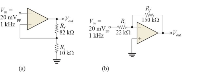 Figure 4 Both op- amps are compensated and have AOL = 100 dB and fT = 2 MHz.
Refer to Figure 4(a). The open- loop critical frequency, fc(ol), is
A)20 Hz
B)2.0 Hz
C)100 Hz
D)10 Hz
Question
 Figure 2
Refer to Figure 2(a). The closed- loop gain, ACL, is
A)+7.8
B)+6.8
C)-6.8
D)-7.8
Question
 Figure 3
Refer to Figure 3. As the closed- loop gain, ACL, increases, the
A)bandwidth decreases
B)input impedance increases
C)CMRR decreases
D)all of the above
Question
Question
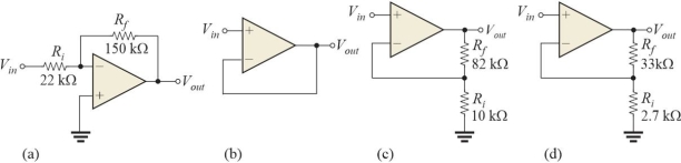 Figure 2
Refer to Figure 2(b). The feedback fraction, B, is
A)+1
B)0
C)-1
D)none of the above
Question
Figure 2Refer to Figure 2(c). The closed- loop gain, ACL, is
A)-9.2
B)+9.2
C)+8.2
D)-8.2
Question
Question
 Figure 5 The RC components shown represent internal R and C of a compensated op- amp.
Refer to Figure 5. Assume the input frequency is much less that fc. In this case, the overall AOL is
A)dependent on the feedback
B)equal to 1
C)halved
D)nearly unaffected
Question
Question
 Figure 2
Refer to Figure 2. The circuit or circuits with a virtual ground is
A)(a)
B)(b)
C)(c)and (d)
D)all of these
Question
Question
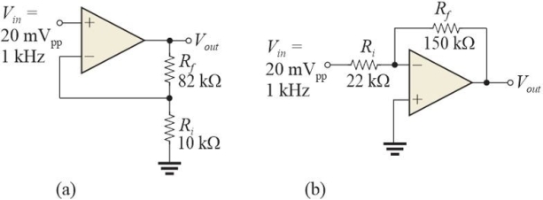 Figure 4 Both op- amps are compensated and have AOL = 100 dB and fT = 2 MHz.
Refer to Figure 4(a). The closed loop bandwidth, fc(cl), is
A)293 kHz
B)344 kHz
C)244 kHz
D)218 kHz
Question
Question
 Figure 4 Both op- amps are compensated and have AOL = 100 dB and fT = 2 MHz.
Refer to Figure 4(a). Assume the output is a 1.0 kHz square wave that goes between +Vmax and -Vmax. This fault is likely due to an
A)open Rf
B)internal open in the op- amp
C)open Ri
D)shorted Ri
Question
Question
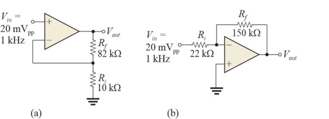 Figure 4 Both op- amps are compensated and have AOL = 100 dB and fT = 2 MHz.
Refer to Figure 4(b). If the feedback resistor is open, the BW will equal
A)fT
B)0
C)fc(ol)
D)none of the above
Question
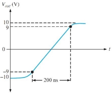 Figure 1
Refer to Figure 1. The signal represents the output of a fast op- amp to a step input voltage. The slew rate for this op- amp is
A)90 V/ µs
B)18 V/ns
C)200 ns
D)45 V/ µs
Question
 Figure 3
Refer to Figure 3. With a constant input, the output ranges from
A)+300 mV to +550 mV
B)-300 mV to -550 mV
C)+250 mV to +500 mV
D)-250 mV to -500 mV
Question
Question
Question
Question
Question
Question
Question
Question
Question
 Figure 4 Both op- amps are compensated and have AOL = 100 dB and fT = 2 MHz.
Refer to Figure 4(b). The closed loop bandwidth, fc(cl), is
A)293 kHz
B)218 kHz
C)244 kHz
D)256 kHz
Question
Question
Question
Question
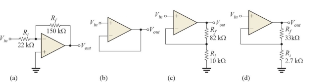 Figure 2
Refer to Figure 2. The circuit with the highest absolute gain, |ACL|, is
A)(a)
B)(b)
C)(c)
D)(d)
Question
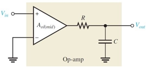 Figure 5 The RC components shown represent internal R and C of a compensated op- amp.
Refer to Figure 5. Assume the input frequency is equal to the critical frequency. The phase shift is
A)-30°
B)-90°
C)0°
D)-45°
Question
Question
Question
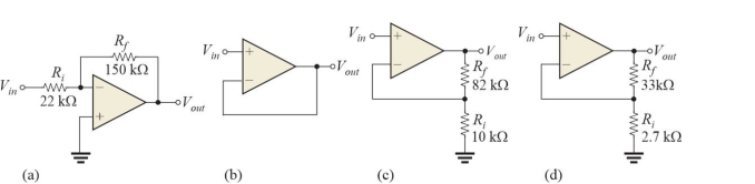 Figure 2
Refer to Figure 2. The circuit with the lowest input impedance is
A)(a)
B)(b)
C)(c)
D)(d)

Unlock Deck
Sign up to unlock the cards in this deck!
Unlock Deck
Unlock Deck
1/36
Play
Full screen (f)
Deck 12: The Operational Amplifier
1
The input offset current, IOS, is the
A)largest of two bias currents
B)sum of two bias currents
C)average of two bias currents
D)difference of two bias currents
A)largest of two bias currents
B)sum of two bias currents
C)average of two bias currents
D)difference of two bias currents
D
2
Figure 4 Both op- amps are compensated and have AOL = 100 dB and fT = 2 MHz.Refer to Figure 4(a). The open- loop critical frequency, fc(ol), is
A)20 Hz
B)2.0 Hz
C)100 Hz
D)10 Hz
A
3
Figure 2Refer to Figure 2(a). The closed- loop gain, ACL, is
A)+7.8
B)+6.8
C)-6.8
D)-7.8
C
4
Figure 3Refer to Figure 3. As the closed- loop gain, ACL, increases, the
A)bandwidth decreases
B)input impedance increases
C)CMRR decreases
D)all of the above
Unlock Deck
Unlock for access to all 36 flashcards in this deck.
Unlock Deck
k this deck
5
The input resistance of a BIFET is
A)low
B)dependent on the load
C)controlled by the bias current
D)none of the above
A)low
B)dependent on the load
C)controlled by the bias current
D)none of the above
Unlock Deck
Unlock for access to all 36 flashcards in this deck.
Unlock Deck
k this deck
6
Figure 2Refer to Figure 2(b). The feedback fraction, B, is
A)+1
B)0
C)-1
D)none of the above
Unlock Deck
Unlock for access to all 36 flashcards in this deck.
Unlock Deck
k this deck
7
Figure 2Refer to Figure 2(c). The closed- loop gain, ACL, is
A)-9.2
B)+9.2
C)+8.2
D)-8.2
Unlock Deck
Unlock for access to all 36 flashcards in this deck.
Unlock Deck
k this deck
8
A typical op- amp
A)uses dc coupling
B)has two supply voltages
C)has very high open- loop gain
D)all of the above
A)uses dc coupling
B)has two supply voltages
C)has very high open- loop gain
D)all of the above
Unlock Deck
Unlock for access to all 36 flashcards in this deck.
Unlock Deck
k this deck
9
Figure 5 The RC components shown represent internal R and C of a compensated op- amp.Refer to Figure 5. Assume the input frequency is much less that fc. In this case, the overall AOL is
A)dependent on the feedback
B)equal to 1
C)halved
D)nearly unaffected
Unlock Deck
Unlock for access to all 36 flashcards in this deck.
Unlock Deck
k this deck
10
Common- mode rejection ratio (CMRR)depends on the
A)input voltage
B)frequency
C)bias current
D)all of the above
A)input voltage
B)frequency
C)bias current
D)all of the above
Unlock Deck
Unlock for access to all 36 flashcards in this deck.
Unlock Deck
k this deck
11
Figure 2Refer to Figure 2. The circuit or circuits with a virtual ground is
A)(a)
B)(b)
C)(c)and (d)
D)all of these
Unlock Deck
Unlock for access to all 36 flashcards in this deck.
Unlock Deck
k this deck
12
When the closed loop gain, ACL, is equal to 0 dB, the bandwidth is
A)the same as at fc
B)minimum
C)maximum
D)none of the above
A)the same as at fc
B)minimum
C)maximum
D)none of the above
Unlock Deck
Unlock for access to all 36 flashcards in this deck.
Unlock Deck
k this deck
13
Figure 4 Both op- amps are compensated and have AOL = 100 dB and fT = 2 MHz.Refer to Figure 4(a). The closed loop bandwidth, fc(cl), is
A)293 kHz
B)344 kHz
C)244 kHz
D)218 kHz
Unlock Deck
Unlock for access to all 36 flashcards in this deck.
Unlock Deck
k this deck
14
The common- mode gain, ACM, of an op- amp with AOL = 200,000 and a CMRR of 80 dB is
A)10
B)40
C)80
D)20
A)10
B)40
C)80
D)20
Unlock Deck
Unlock for access to all 36 flashcards in this deck.
Unlock Deck
k this deck
15
Figure 4 Both op- amps are compensated and have AOL = 100 dB and fT = 2 MHz.Refer to Figure 4(a). Assume the output is a 1.0 kHz square wave that goes between +Vmax and -Vmax. This fault is likely due to an
A)open Rf
B)internal open in the op- amp
C)open Ri
D)shorted Ri
Unlock Deck
Unlock for access to all 36 flashcards in this deck.
Unlock Deck
k this deck
16
A CMRR of 110,000 is expressed in dB as
A)50.4 dB
B)106 dB
C)101 dB
D)110 dB
A)50.4 dB
B)106 dB
C)101 dB
D)110 dB
Unlock Deck
Unlock for access to all 36 flashcards in this deck.
Unlock Deck
k this deck
17
Figure 4 Both op- amps are compensated and have AOL = 100 dB and fT = 2 MHz.Refer to Figure 4(b). If the feedback resistor is open, the BW will equal
A)fT
B)0
C)fc(ol)
D)none of the above
Unlock Deck
Unlock for access to all 36 flashcards in this deck.
Unlock Deck
k this deck
18
Figure 1Refer to Figure 1. The signal represents the output of a fast op- amp to a step input voltage. The slew rate for this op- amp is
A)90 V/ µs
B)18 V/ns
C)200 ns
D)45 V/ µs
Unlock Deck
Unlock for access to all 36 flashcards in this deck.
Unlock Deck
k this deck
19
Figure 3Refer to Figure 3. With a constant input, the output ranges from
A)+300 mV to +550 mV
B)-300 mV to -550 mV
C)+250 mV to +500 mV
D)-250 mV to -500 mV
Unlock Deck
Unlock for access to all 36 flashcards in this deck.
Unlock Deck
k this deck
20
The input offset voltage is defined as a differential input dc voltage that
A)is required to balance the positive and negative supply voltages
B)forces the output to 0 V
C)is the difference in two bias voltages
D)is required to balance the two bias currents
A)is required to balance the positive and negative supply voltages
B)forces the output to 0 V
C)is the difference in two bias voltages
D)is required to balance the two bias currents
Unlock Deck
Unlock for access to all 36 flashcards in this deck.
Unlock Deck
k this deck
21
Differential input impedance is measured from one input to ground.
Unlock Deck
Unlock for access to all 36 flashcards in this deck.
Unlock Deck
k this deck
22
The need for bias current compensation is reduced by
A)using a smaller input signal
B)using a BIFET op- amp
C)using a larger load
D)all of the above
A)using a smaller input signal
B)using a BIFET op- amp
C)using a larger load
D)all of the above
Unlock Deck
Unlock for access to all 36 flashcards in this deck.
Unlock Deck
k this deck
23
The open- loop gain is determined by the feedback circuit.
Unlock Deck
Unlock for access to all 36 flashcards in this deck.
Unlock Deck
k this deck
24
The input stage of an op- amp is a differential amplifier.
Unlock Deck
Unlock for access to all 36 flashcards in this deck.
Unlock Deck
k this deck
25
A common- mode input is when two equal amplitude but opposite polarity signals are applied to the inputs of a differential amplifier.
Unlock Deck
Unlock for access to all 36 flashcards in this deck.
Unlock Deck
k this deck
26
Assume an op- amp has three different internal critical frequencies that are above the fT. The overall roll- off rate is
A)a constant -60 dB/decade
B)a composite of the three critical frequencies
C)the average of the three critical frequencies
D)a constant -20 dB/decade
A)a constant -60 dB/decade
B)a composite of the three critical frequencies
C)the average of the three critical frequencies
D)a constant -20 dB/decade
Unlock Deck
Unlock for access to all 36 flashcards in this deck.
Unlock Deck
k this deck
27
The gain- bandwidth product for a compensated op- amp is a constant.
Unlock Deck
Unlock for access to all 36 flashcards in this deck.
Unlock Deck
k this deck
28
Figure 4 Both op- amps are compensated and have AOL = 100 dB and fT = 2 MHz.Refer to Figure 4(b). The closed loop bandwidth, fc(cl), is
A)293 kHz
B)218 kHz
C)244 kHz
D)256 kHz
Unlock Deck
Unlock for access to all 36 flashcards in this deck.
Unlock Deck
k this deck
29
The open- loop and closed- loop gains for a voltage follower equal 1.
Unlock Deck
Unlock for access to all 36 flashcards in this deck.
Unlock Deck
k this deck
30
The output impedance of an inverting amplifier is very small.
Unlock Deck
Unlock for access to all 36 flashcards in this deck.
Unlock Deck
k this deck
31
CMRR is the ratio of
A)differential open- loop gain to differential closed loop gain
B)inverting open- loop gain to inverting closed- loop gain
C)differential open- loop gain to common mode gain
D)inverting closed- loop gain to common mode gain
A)differential open- loop gain to differential closed loop gain
B)inverting open- loop gain to inverting closed- loop gain
C)differential open- loop gain to common mode gain
D)inverting closed- loop gain to common mode gain
Unlock Deck
Unlock for access to all 36 flashcards in this deck.
Unlock Deck
k this deck
32
Figure 2Refer to Figure 2. The circuit with the highest absolute gain, |ACL|, is
A)(a)
B)(b)
C)(c)
D)(d)
Unlock Deck
Unlock for access to all 36 flashcards in this deck.
Unlock Deck
k this deck
33
Figure 5 The RC components shown represent internal R and C of a compensated op- amp.Refer to Figure 5. Assume the input frequency is equal to the critical frequency. The phase shift is
A)-30°
B)-90°
C)0°
D)-45°
Unlock Deck
Unlock for access to all 36 flashcards in this deck.
Unlock Deck
k this deck
34
At low frequencies, voltage noise density goes up.
Unlock Deck
Unlock for access to all 36 flashcards in this deck.
Unlock Deck
k this deck
35
Assume an op- amp has bias currents of 10.0 µA and 10.2 µA. The input offset current is
A)20.2 µA
B)0.2 µA
C)10.1 µA
D)none of the above
A)20.2 µA
B)0.2 µA
C)10.1 µA
D)none of the above
Unlock Deck
Unlock for access to all 36 flashcards in this deck.
Unlock Deck
k this deck
36
Figure 2Refer to Figure 2. The circuit with the lowest input impedance is
A)(a)
B)(b)
C)(c)
D)(d)
Unlock Deck
Unlock for access to all 36 flashcards in this deck.
Unlock Deck
k this deck
Unlock Deck
Unlock for access to all 36 flashcards in this deck.


