Deck 6: Bjt Amplifiers
Full screen (f)
Question
Question
Question
Question
Question

Refer to the figure above. If VE = 0, the trouble might be that
A)RC is open.
B)RE is open.
C)R1 is open.
D)R2 is open.
Question
Question
Question
Question

Refer to the figure above. The output signal at the collector of Q1 is higher than normal. This could be caused by an)
A)open C1.
B)open base- emitter of Q1.
C)open C3.
D)open C2.
Question

Refer to the figure above. If the collector opened internally, the voltage on the collector would
A)remain the same.
B)decrease.
C)increase.
D)be undetermined.
Question
Question
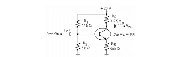
Refer to the figure above. If R2 opened, the value of IC would be
A)8 mA.
B)6 mA.
C)6.67 mA.
D)10 mA.
Question
Question
Question
Question
Question
Question

Refer to the figure above. If R2 opened, VCE would be
A)4.8 V.
B)0 V.
C)20 V.
D)10 V.
Question
Refer to the figure above. If an emitter- bypass capacitor were installed, AV would be
A)4.96.
B)398.
C)125.
D)560.
Question
Question
Question
Question
Question
Question
Question
Question
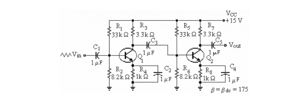
Refer to the figure above. Which of the following faults would account for the output voltage being lower than normal, but not a complete loss of output voltage?
A)An open C4
B)An open C1
C)An open C5
D)An open C3
Question
Question
Question
Question
Question
Question
Question
Question
Question
Question
Question
Question
Question
Question

Refer to the figure above. If AV1 = 75 and AV2 = 95, AVT would be
A)7125.
B)95.
C)75.
D)1275.
Question
Question
Question
Question
Question
Question
Question

Unlock Deck
Sign up to unlock the cards in this deck!
Unlock Deck
Unlock Deck
1/48
Play
Full screen (f)
Deck 6: Bjt Amplifiers
1
If a CE stage is direct coupled to an emitter- follower, how many coupling capacitors are there between the two stages?
A)0
B)1
C)2
D)3
A)0
B)1
C)2
D)3
A
2
Output resistance in a common- collector amplifier circuit is stepped down by a factor of
A)Beta fi.
B)r'e + re.
C)alpha a.
D)RE "RL.
A)Beta fi.
B)r'e + re.
C)alpha a.
D)RE "RL.
A
3
A three- stage amplifier has a gain of 20 for each stage. The overall decibel voltage gain is
A)78 dB.
B)60 dB.
C)400 dB.
D)8,000 dB.
A)78 dB.
B)60 dB.
C)400 dB.
D)8,000 dB.
A
4
The best choice for a very high power amplifier is an)
A)common- base.
B)common- emitter.
C)common- collector.
D)emitter- follower.
A)common- base.
B)common- emitter.
C)common- collector.
D)emitter- follower.
Unlock Deck
Unlock for access to all 48 flashcards in this deck.
Unlock Deck
k this deck
5
Refer to the figure above. If VE = 0, the trouble might be that
A)RC is open.
B)RE is open.
C)R1 is open.
D)R2 is open.
Unlock Deck
Unlock for access to all 48 flashcards in this deck.
Unlock Deck
k this deck
6
The voltage gain of a common- emitter amplifier, AV, can be defined as
A)AV = IeRC .
B)AV = Vb .
C)AV = IC × RC.
D)AV = RC .
A)AV = IeRC .
B)AV = Vb .
C)AV = IC × RC.
D)AV = RC .
Unlock Deck
Unlock for access to all 48 flashcards in this deck.
Unlock Deck
k this deck
7
A differential amplifier should exhibit a differential gain and a common mode gain.
A)low, high
B)high, high
C)high, low
D)low, low
A)low, high
B)high, high
C)high, low
D)low, low
Unlock Deck
Unlock for access to all 48 flashcards in this deck.
Unlock Deck
k this deck
8
The input resistance, Rinbase), of a common- emitter amplifier, consists of
A)RG " rc " fir'e.
B)re " fir'e.
C)fiac r'e.
D)rb " fire.
A)RG " rc " fir'e.
B)re " fir'e.
C)fiac r'e.
D)rb " fire.
Unlock Deck
Unlock for access to all 48 flashcards in this deck.
Unlock Deck
k this deck
9
Refer to the figure above. The output signal at the collector of Q1 is higher than normal. This could be caused by an)
A)open C1.
B)open base- emitter of Q1.
C)open C3.
D)open C2.
Unlock Deck
Unlock for access to all 48 flashcards in this deck.
Unlock Deck
k this deck
10
Refer to the figure above. If the collector opened internally, the voltage on the collector would
A)remain the same.
B)decrease.
C)increase.
D)be undetermined.
Unlock Deck
Unlock for access to all 48 flashcards in this deck.
Unlock Deck
k this deck
11
Assume that a certain differential amplifier has a differential gain of 5,000 and a common mode gain of 0.3. What is the CMRR in dB?
A)1,500 dB
B)84.44 dB
C)0.3 dB
D)62.12 dB
A)1,500 dB
B)84.44 dB
C)0.3 dB
D)62.12 dB
Unlock Deck
Unlock for access to all 48 flashcards in this deck.
Unlock Deck
k this deck
12
Refer to the figure above. If R2 opened, the value of IC would be
A)8 mA.
B)6 mA.
C)6.67 mA.
D)10 mA.
Unlock Deck
Unlock for access to all 48 flashcards in this deck.
Unlock Deck
k this deck
13
A differential amplifier provides an output that is the _ _ of the two input quantities.
A)sine
B)difference
C)square
D)multiplication
A)sine
B)difference
C)square
D)multiplication
Unlock Deck
Unlock for access to all 48 flashcards in this deck.
Unlock Deck
k this deck
14
To reduce the distortion of an amplified signal, you can increase the
A)load resistance.
B)emitter feedback resistance.
C)generator resistance.
D)collector resistance.
A)load resistance.
B)emitter feedback resistance.
C)generator resistance.
D)collector resistance.
Unlock Deck
Unlock for access to all 48 flashcards in this deck.
Unlock Deck
k this deck
15
Assume that a certain differential amplifier has a differential gain of 3,000 and a common mode gain of 0.25. What is the CMRR?
A)12,000
B)66.89
C)750
D)3,025
A)12,000
B)66.89
C)750
D)3,025
Unlock Deck
Unlock for access to all 48 flashcards in this deck.
Unlock Deck
k this deck
16
The capacitor that produces an ac ground at a point in a circuit is called an)
A)ac open.
B)dc short.
C)coupling capacitor.
D)bypass capacitor.
A)ac open.
B)dc short.
C)coupling capacitor.
D)bypass capacitor.
Unlock Deck
Unlock for access to all 48 flashcards in this deck.
Unlock Deck
k this deck
17
The input resistance of the base of an emitter follower is usually
A)low.
B)shorted to ground.
C)high.
D)open.
A)low.
B)shorted to ground.
C)high.
D)open.
Unlock Deck
Unlock for access to all 48 flashcards in this deck.
Unlock Deck
k this deck
18
Refer to the figure above. If R2 opened, VCE would be
A)4.8 V.
B)0 V.
C)20 V.
D)10 V.
Unlock Deck
Unlock for access to all 48 flashcards in this deck.
Unlock Deck
k this deck
19
Refer to the figure above. If an emitter- bypass capacitor were installed, AV would be
A)4.96.
B)398.
C)125.
D)560.
Unlock Deck
Unlock for access to all 48 flashcards in this deck.
Unlock Deck
k this deck
20
Which of the following is not a characteristic of the emitter- follower?
A)Low output impedance
B)Low input impedance
C)High current gain
D)Voltage gain of 1
A)Low output impedance
B)Low input impedance
C)High current gain
D)Voltage gain of 1
Unlock Deck
Unlock for access to all 48 flashcards in this deck.
Unlock Deck
k this deck
21
Removing the emitter bypass capacitor from a common- emitter amplifier
A)increases the distortion.
B)does not affect Rin.
C)decreases Rin and increases voltage gain.
D)increases Rin and decreases voltage gain.
A)increases the distortion.
B)does not affect Rin.
C)decreases Rin and increases voltage gain.
D)increases Rin and decreases voltage gain.
Unlock Deck
Unlock for access to all 48 flashcards in this deck.
Unlock Deck
k this deck
22
For a bypass capacitor to work properly, the
A)XC should be ten times greater than RE at the minimum operating frequency.
B)XC should be ten times smaller than RE at the minimum operating frequency.
C)XC should equal RE.
D)XC should be twice the value of the RE.
A)XC should be ten times greater than RE at the minimum operating frequency.
B)XC should be ten times smaller than RE at the minimum operating frequency.
C)XC should equal RE.
D)XC should be twice the value of the RE.
Unlock Deck
Unlock for access to all 48 flashcards in this deck.
Unlock Deck
k this deck
23
Removing a bypass capacitor from a fully bypassed, common- emitter amplifier circuit will voltage gain and ac input resistance.
A)decrease, decrease
B)increase, decrease
C)decrease, increase
D)increase, increase
A)decrease, decrease
B)increase, decrease
C)decrease, increase
D)increase, increase
Unlock Deck
Unlock for access to all 48 flashcards in this deck.
Unlock Deck
k this deck
24
The voltage gain of an amplifier is defined as the
A)ac collector current divided by the ac emitter current.
B)ac input voltage divided by the ac output voltage.
C)ac collector current divided by the ac base current.
D)ac output voltage divided by the ac input voltage.
A)ac collector current divided by the ac emitter current.
B)ac input voltage divided by the ac output voltage.
C)ac collector current divided by the ac base current.
D)ac output voltage divided by the ac input voltage.
Unlock Deck
Unlock for access to all 48 flashcards in this deck.
Unlock Deck
k this deck
25
The value of output resistance in a common- emitter amplifier, Rout, consists of
A)RL + RC.
B)fi " RC.
C)RC.
D)RL " RC.
A)RL + RC.
B)fi " RC.
C)RC.
D)RL " RC.
Unlock Deck
Unlock for access to all 48 flashcards in this deck.
Unlock Deck
k this deck
26
In a two- stage amplifier, the voltage gain of the first stage is 80 and the voltage gain of the second stage is 50. How much is the overall voltage gain?
A)400
B)130
C)4,000
D)72
A)400
B)130
C)4,000
D)72
Unlock Deck
Unlock for access to all 48 flashcards in this deck.
Unlock Deck
k this deck
27
Refer to the figure above. Which of the following faults would account for the output voltage being lower than normal, but not a complete loss of output voltage?
A)An open C4
B)An open C1
C)An open C5
D)An open C3
Unlock Deck
Unlock for access to all 48 flashcards in this deck.
Unlock Deck
k this deck
28
For transistors
A)the dc and ac current gains are the same.
B)amplification of signal voltage is not possible.
C)the dc and ac current gains are usually different.
D)the dc current gain is zero.
A)the dc and ac current gains are the same.
B)amplification of signal voltage is not possible.
C)the dc and ac current gains are usually different.
D)the dc current gain is zero.
Unlock Deck
Unlock for access to all 48 flashcards in this deck.
Unlock Deck
k this deck
29
Leaving some of the emitter resistance unbypassed in a common- emitter amplifier will
A)reduce distortion.
B)increase the input impedance.
C)stabilize the voltage gain.
D)All of the above.
A)reduce distortion.
B)increase the input impedance.
C)stabilize the voltage gain.
D)All of the above.
Unlock Deck
Unlock for access to all 48 flashcards in this deck.
Unlock Deck
k this deck
30
The best selection for a high input impedance amplifier is a
A)high gain common- emitter.
B)common- base.
C)low gain common- emitter.
D)common- collector.
A)high gain common- emitter.
B)common- base.
C)low gain common- emitter.
D)common- collector.
Unlock Deck
Unlock for access to all 48 flashcards in this deck.
Unlock Deck
k this deck
31
In a swamped amplifier, the effects of r'e become
A)significant to the analysis.
B)insignificant.
C)important to voltage gain.
D)critical to input impedance.
A)significant to the analysis.
B)insignificant.
C)important to voltage gain.
D)critical to input impedance.
Unlock Deck
Unlock for access to all 48 flashcards in this deck.
Unlock Deck
k this deck
32
If two transistors are connected as a Darlington pair and each transistor has a Beta of 175, the overall current gain of the pair equals
A)5,000.
B)3,625.
C)10,000.
D)30,625.
A)5,000.
B)3,625.
C)10,000.
D)30,625.
Unlock Deck
Unlock for access to all 48 flashcards in this deck.
Unlock Deck
k this deck
33
Where is the output coupling capacitor connected on a common- collector amplifier?
A)Emitter
B)Collector
C)dc power supply
D)Base
A)Emitter
B)Collector
C)dc power supply
D)Base
Unlock Deck
Unlock for access to all 48 flashcards in this deck.
Unlock Deck
k this deck
34
A certain transistor has a dc emitter current of 25 mA. The value of r'e is
A)1 ▲.
B)2.5 ▲.
C)1.2 ▲.
D)25 ▲.
A)1 ▲.
B)2.5 ▲.
C)1.2 ▲.
D)25 ▲.
Unlock Deck
Unlock for access to all 48 flashcards in this deck.
Unlock Deck
k this deck
35
A bypass capacitor is placed across the emitter resistor in a voltage- divider biased common- emitter amplifier circuit. This will
A)place the emitter at ac ground.
B)reduce the emitter's dc voltage to zero.
C)shift the Q- point on the dc load line.
D)All of the above.
A)place the emitter at ac ground.
B)reduce the emitter's dc voltage to zero.
C)shift the Q- point on the dc load line.
D)All of the above.
Unlock Deck
Unlock for access to all 48 flashcards in this deck.
Unlock Deck
k this deck
36
The quantity r'e
A)is a dc value.
B)is temperature dependent.
C)is external to the transistor.
D)has no effect on gain in transistors.
A)is a dc value.
B)is temperature dependent.
C)is external to the transistor.
D)has no effect on gain in transistors.
Unlock Deck
Unlock for access to all 48 flashcards in this deck.
Unlock Deck
k this deck
37
In general, coupling capacitors can be considered
A)open for signal voltage and a short for dc.
B)lossy.
C)short for signal voltage and an open for dc.
D)short for signal voltage and a short for dc.
A)open for signal voltage and a short for dc.
B)lossy.
C)short for signal voltage and an open for dc.
D)short for signal voltage and a short for dc.
Unlock Deck
Unlock for access to all 48 flashcards in this deck.
Unlock Deck
k this deck
38
Reducing all dc sources to zero is done to help obtain the
A)complete amplifier circuit.
B)dc equivalent circuit.
C)voltage- divider biased circuit.
D)ac equivalent circuit.
A)complete amplifier circuit.
B)dc equivalent circuit.
C)voltage- divider biased circuit.
D)ac equivalent circuit.
Unlock Deck
Unlock for access to all 48 flashcards in this deck.
Unlock Deck
k this deck
39
An emitter follower has a voltage gain that is
A)much less than one.
B)zero.
C)approximately equal to one.
D)greater than one.
A)much less than one.
B)zero.
C)approximately equal to one.
D)greater than one.
Unlock Deck
Unlock for access to all 48 flashcards in this deck.
Unlock Deck
k this deck
40
The primary reason an ac load line differs from a dc load line is
A)changes in current are nonlinear for small- signal amplifier operation.
B)the ac load line is not as steep as the dc load line.
C)the effective ac collector resistance is greater than the dc collector resistance.
D)the effective ac collector resistance is less than the dc collector resistance.
A)changes in current are nonlinear for small- signal amplifier operation.
B)the ac load line is not as steep as the dc load line.
C)the effective ac collector resistance is greater than the dc collector resistance.
D)the effective ac collector resistance is less than the dc collector resistance.
Unlock Deck
Unlock for access to all 48 flashcards in this deck.
Unlock Deck
k this deck
41
Refer to the figure above. If AV1 = 75 and AV2 = 95, AVT would be
A)7125.
B)95.
C)75.
D)1275.
Unlock Deck
Unlock for access to all 48 flashcards in this deck.
Unlock Deck
k this deck
42
The three factors that must be taken into account when determining the actual signal voltage at the base of a small signal bipolar amplifier are
A)source resistance, bias resistance, and input resistance.
B)source resistance, collector resistance, internal resistance.
C)source resistance, emitter resistance, and input resistance.
D)source resistance, bias resistance, and load resistance.
A)source resistance, bias resistance, and input resistance.
B)source resistance, collector resistance, internal resistance.
C)source resistance, emitter resistance, and input resistance.
D)source resistance, bias resistance, and load resistance.
Unlock Deck
Unlock for access to all 48 flashcards in this deck.
Unlock Deck
k this deck
43
The h- parameter, hfe, is the same as of the transistor.
A)ac Beta
B)minimum hold current
C)maximum collector current
D)dc Beta
A)ac Beta
B)minimum hold current
C)maximum collector current
D)dc Beta
Unlock Deck
Unlock for access to all 48 flashcards in this deck.
Unlock Deck
k this deck
44
Increasing the resistance of the load resistor in an RC coupled common- emitter amplifier will have what effect on voltage gain?
A)Increases the voltage gain
B)Decreases the voltage gain
C)Does not affect the voltage gain
A)Increases the voltage gain
B)Decreases the voltage gain
C)Does not affect the voltage gain
Unlock Deck
Unlock for access to all 48 flashcards in this deck.
Unlock Deck
k this deck
45
Often a common- collector will be the last stage before the load; the main functions)of this stage is to
A)provide a high frequency path to improve the frequency response.
B)provide a large voltage gain.
C)buffer the voltage amplifiers from the low resistance load and provide impedance matching for maximum power transfer.
D)provide phase inversion.
A)provide a high frequency path to improve the frequency response.
B)provide a large voltage gain.
C)buffer the voltage amplifiers from the low resistance load and provide impedance matching for maximum power transfer.
D)provide phase inversion.
Unlock Deck
Unlock for access to all 48 flashcards in this deck.
Unlock Deck
k this deck
46
Which of the following is not a characteristic of the common- base amplifier?
A)High voltage gain
B)High input impedance
C)Current gain of 1
D)High output impedance
A)High voltage gain
B)High input impedance
C)Current gain of 1
D)High output impedance
Unlock Deck
Unlock for access to all 48 flashcards in this deck.
Unlock Deck
k this deck
47
The ac resistance r'e approximately equals
A)25 mV .
B)25 mV .
C)25 mV .
D)25 mV × IC. IB IC IE
A)25 mV .
B)25 mV .
C)25 mV .
D)25 mV × IC. IB IC IE
Unlock Deck
Unlock for access to all 48 flashcards in this deck.
Unlock Deck
k this deck
48
In a two- stage amplifier, the input resistance of the second stage
A)does not affect the voltage gain of the first stage.
B)affects the voltage gain of the first stage.
C)is in parallel with the collector resistor of the first stage.
D)Both B and C above.
A)does not affect the voltage gain of the first stage.
B)affects the voltage gain of the first stage.
C)is in parallel with the collector resistor of the first stage.
D)Both B and C above.
Unlock Deck
Unlock for access to all 48 flashcards in this deck.
Unlock Deck
k this deck
Unlock Deck
Unlock for access to all 48 flashcards in this deck.


