Deck 8: Field-Effect Transistors Fets
Full screen (f)
Question

Refer to b)in the figure above. If ID = 4 mA, the value of VGS is
A)0 V.
B)11.2 V.
C)8.8 V.
D)20 V.
Question
Question
Question
Question
Question
Question
Question
Question
Question
Question
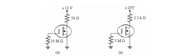
Refer to b)in the figure above. If ID = 2 mA, the value of VDS is
A)10 V.
B)20 V.
C)4.4 V.
D)15.6 V.
Question
Question
Question
Question

Refer to c)in the figure above. This symbol identifies
A)an n-channel E- MOSFET.
B)a p-channel D- MOSFET.
C)a p-channel E- MOSFET.
D)an n-channel D- MOSFET.
Question
Question
Question
Refer to a)in the figure above. This symbol identifies
A)a p-channel D- MOSFET.
B)an n-channel E- MOSFET.
C)an n-channel D- MOSFET.
D)a p-channel E- MOSFET.
Question

Refer to the figure above. In this circuit, VGS is biased correctly for proper operation. This means that VGS is
A)0 V.
B)positive.
C)negative.
D)either negative or positive.
Question
Question
Question
Question
Refer to b)in the figure above. This symbol identifies
A)a p-channel D- MOSFET.
B)a p-channel E- MOSFET.
C)an n-channel D- MOSFET.
D)an n-channel E- MOSFET.
Question
Question
Question
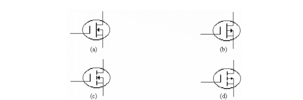
Refer to d)in the figure above. This symbol identifies
A)a p-channel E- MOSFET.
B)a p-channel D- MOSFET.
C)an n-channel E- MOSFET.
D)an n-channel D- MOSFET.
Question
Question

Refer to a)in the figure above. If ID = 4 mA, the value of VDS is
A)12 V.
B)0 V.
C)4 V.
D)8 V.
Question
Question
Question
Question
Question
Question
Question
Question
Question

Unlock Deck
Sign up to unlock the cards in this deck!
Unlock Deck
Unlock Deck
1/37
Play
Full screen (f)
Deck 8: Field-Effect Transistors Fets
1
Refer to b)in the figure above. If ID = 4 mA, the value of VGS is
A)0 V.
B)11.2 V.
C)8.8 V.
D)20 V.
A
2
The types)of bias most often used with E- MOSFET circuits is
A)drain- feedback.
B)constant current.
C)voltage- divider.
D)Both A and C above.
A)drain- feedback.
B)constant current.
C)voltage- divider.
D)Both A and C above.
D
3
To get a negative gate- source voltage in a self- biased JFET circuit, you must use a
A)source resistor.
B)negative gate supply voltage.
C)voltage divider.
D)ground.
A)source resistor.
B)negative gate supply voltage.
C)voltage divider.
D)ground.
A
4
The transconductance curve of a JFET is
A)linear.
B)hyperbolic.
C)nonlinear.
D)symmetrical.
A)linear.
B)hyperbolic.
C)nonlinear.
D)symmetrical.
Unlock Deck
Unlock for access to all 37 flashcards in this deck.
Unlock Deck
k this deck
5
The transconductance curve of a JFET is a graph of
A)ID × RDS.
B)IC versus VCE.
C)IS versus VDS.
D)ID versus VGS.
A)ID × RDS.
B)IC versus VCE.
C)IS versus VDS.
D)ID versus VGS.
Unlock Deck
Unlock for access to all 37 flashcards in this deck.
Unlock Deck
k this deck
6
A V- MOSFET device operates in
A)a JFET mode.
B)the enhancement mode.
C)the depletion mode.
D)in either enhancement or depletion mode.
A)a JFET mode.
B)the enhancement mode.
C)the depletion mode.
D)in either enhancement or depletion mode.
Unlock Deck
Unlock for access to all 37 flashcards in this deck.
Unlock Deck
k this deck
7
The FET that has no physical channel is
A)the E- MOSFET.
B)the JFET.
C)the D- MOSFET.
D)None of the above.
A)the E- MOSFET.
B)the JFET.
C)the D- MOSFET.
D)None of the above.
Unlock Deck
Unlock for access to all 37 flashcards in this deck.
Unlock Deck
k this deck
8
Special handling precautions should be taken when working with MOSFETs. Which of the following is not one of these precautions?
A)Workers handling MOSFET devices should not have grounding straps attached to their wrists.
B)All test equipment should be grounded.
C)MOSFET devices should have their leads shorted together for shipment and storage.
D)Never remove or insert MOSFET devices with the power on.
A)Workers handling MOSFET devices should not have grounding straps attached to their wrists.
B)All test equipment should be grounded.
C)MOSFET devices should have their leads shorted together for shipment and storage.
D)Never remove or insert MOSFET devices with the power on.
Unlock Deck
Unlock for access to all 37 flashcards in this deck.
Unlock Deck
k this deck
9
IDSS can be defined as the
A)maximum possible current with the drain shorted to the source.
B)minimum possible drain current.
C)maximum current drain- to- source with a shorted gate.
D)maximum drain current with the source shorted.
A)maximum possible current with the drain shorted to the source.
B)minimum possible drain current.
C)maximum current drain- to- source with a shorted gate.
D)maximum drain current with the source shorted.
Unlock Deck
Unlock for access to all 37 flashcards in this deck.
Unlock Deck
k this deck
10
The pinch- off voltage has the same magnitude as the
A)gate voltage.
B)gate- source voltage.
C)gate- source cutoff voltage.
D)drain- source voltage.
A)gate voltage.
B)gate- source voltage.
C)gate- source cutoff voltage.
D)drain- source voltage.
Unlock Deck
Unlock for access to all 37 flashcards in this deck.
Unlock Deck
k this deck
11
Refer to b)in the figure above. If ID = 2 mA, the value of VDS is
A)10 V.
B)20 V.
C)4.4 V.
D)15.6 V.
Unlock Deck
Unlock for access to all 37 flashcards in this deck.
Unlock Deck
k this deck
12
One advantage of voltage- divider bias is that the dependency of drain current ID, on the range of Q- points is
A)reduced.
B)not affected.
C)increased.
A)reduced.
B)not affected.
C)increased.
Unlock Deck
Unlock for access to all 37 flashcards in this deck.
Unlock Deck
k this deck
13
VDS equals pinch- off voltage divided by the
A)base current.
B)drain current for zero gate voltage.
C)gate current.
D)ideal drain current.
A)base current.
B)drain current for zero gate voltage.
C)gate current.
D)ideal drain current.
Unlock Deck
Unlock for access to all 37 flashcards in this deck.
Unlock Deck
k this deck
14
A self- biased n-channel JFET has a VD = 8 V, VGS = - 5 V. The value of VDS is
A)- 5 V.
B)- 3 V.
C)8 V.
D)3 V.
A)- 5 V.
B)- 3 V.
C)8 V.
D)3 V.
Unlock Deck
Unlock for access to all 37 flashcards in this deck.
Unlock Deck
k this deck
15
Refer to c)in the figure above. This symbol identifies
A)an n-channel E- MOSFET.
B)a p-channel D- MOSFET.
C)a p-channel E- MOSFET.
D)an n-channel D- MOSFET.
Unlock Deck
Unlock for access to all 37 flashcards in this deck.
Unlock Deck
k this deck
16
An IGBT has the output characteristics of a but is - controlled like a MOSFET.
A)FET, voltage
B)BJT, voltage
C)FET, current
D)BJT, current
A)FET, voltage
B)BJT, voltage
C)FET, current
D)BJT, current
Unlock Deck
Unlock for access to all 37 flashcards in this deck.
Unlock Deck
k this deck
17
A FET that has no IDSS parameter is the
A)DE- MOSFET.
B)E- MOSFET.
C)V- MOSFET.
D)JFET.
A)DE- MOSFET.
B)E- MOSFET.
C)V- MOSFET.
D)JFET.
Unlock Deck
Unlock for access to all 37 flashcards in this deck.
Unlock Deck
k this deck
18
Refer to a)in the figure above. This symbol identifies
A)a p-channel D- MOSFET.
B)an n-channel E- MOSFET.
C)an n-channel D- MOSFET.
D)a p-channel E- MOSFET.
Unlock Deck
Unlock for access to all 37 flashcards in this deck.
Unlock Deck
k this deck
19
Refer to the figure above. In this circuit, VGS is biased correctly for proper operation. This means that VGS is
A)0 V.
B)positive.
C)negative.
D)either negative or positive.
Unlock Deck
Unlock for access to all 37 flashcards in this deck.
Unlock Deck
k this deck
20
The easiest way to bias a JFET in the ohmic region is with
A)self- bias.
B)voltage- divider bias.
C)gate bias.
D)source bias.
A)self- bias.
B)voltage- divider bias.
C)gate bias.
D)source bias.
Unlock Deck
Unlock for access to all 37 flashcards in this deck.
Unlock Deck
k this deck
21
The gate- source junction of a JFET is
A)normally reverse- biased.
B)normally not biased.
C)a low resistance path for dc current when reverse- biased.
D)normally forward- biased.
A)normally reverse- biased.
B)normally not biased.
C)a low resistance path for dc current when reverse- biased.
D)normally forward- biased.
Unlock Deck
Unlock for access to all 37 flashcards in this deck.
Unlock Deck
k this deck
22
The simplest method to bias a D- MOSFET is to
A)set VGS = 0.
B)select the correct value RD.
C)set VGS = - 4.
D)set VGS = +4.
A)set VGS = 0.
B)select the correct value RD.
C)set VGS = - 4.
D)set VGS = +4.
Unlock Deck
Unlock for access to all 37 flashcards in this deck.
Unlock Deck
k this deck
23
Refer to b)in the figure above. This symbol identifies
A)a p-channel D- MOSFET.
B)a p-channel E- MOSFET.
C)an n-channel D- MOSFET.
D)an n-channel E- MOSFET.
Unlock Deck
Unlock for access to all 37 flashcards in this deck.
Unlock Deck
k this deck
24
JFETs are often called
A)one- way switches.
B)unipolar devices.
C)bipolar devices.
D)two- way switches.
A)one- way switches.
B)unipolar devices.
C)bipolar devices.
D)two- way switches.
Unlock Deck
Unlock for access to all 37 flashcards in this deck.
Unlock Deck
k this deck
25
For a JFET, there is maximum drain current when
A)VDS is zero.
B)VGS is zero.
C)the drain and source are interchanged.
D)VGS equals VGSoff).
A)VDS is zero.
B)VGS is zero.
C)the drain and source are interchanged.
D)VGS equals VGSoff).
Unlock Deck
Unlock for access to all 37 flashcards in this deck.
Unlock Deck
k this deck
26
Refer to d)in the figure above. This symbol identifies
A)a p-channel E- MOSFET.
B)a p-channel D- MOSFET.
C)an n-channel E- MOSFET.
D)an n-channel D- MOSFET.
Unlock Deck
Unlock for access to all 37 flashcards in this deck.
Unlock Deck
k this deck
27
A JFET manufacturer's data sheet specifies VGSoff)= - 8 V and IDSS = 6 mA. When VGS = - 4 V, the value of ID would be
A)4 mA.
B)1.5 mA.
C)1.25 mA.
D)6 mA.
A)4 mA.
B)1.5 mA.
C)1.25 mA.
D)6 mA.
Unlock Deck
Unlock for access to all 37 flashcards in this deck.
Unlock Deck
k this deck
28
Refer to a)in the figure above. If ID = 4 mA, the value of VDS is
A)12 V.
B)0 V.
C)4 V.
D)8 V.
Unlock Deck
Unlock for access to all 37 flashcards in this deck.
Unlock Deck
k this deck
29
The depletion- mode MOSFET can
A)operate with positive as well as negative gate voltages.
B)operate with only positive gate voltages.
C)not operate in the ohmic region.
D)operate with only negative gate voltages.
A)operate with positive as well as negative gate voltages.
B)operate with only positive gate voltages.
C)not operate in the ohmic region.
D)operate with only negative gate voltages.
Unlock Deck
Unlock for access to all 37 flashcards in this deck.
Unlock Deck
k this deck
30
A good application for a V- MOSFET would be as a
A)low power amplifier.
B)substitute for a diode.
C)low input impedance device.
D)power amplifier.
A)low power amplifier.
B)substitute for a diode.
C)low input impedance device.
D)power amplifier.
Unlock Deck
Unlock for access to all 37 flashcards in this deck.
Unlock Deck
k this deck
31
An n-channel E- MOSFET conducts when it has
A)VGS > VP.
B)a thin layer of positive charges in the substrate region near the SiO2 layer.
C)a thin layer of negative charges in the substrate region near the SiO2 layer.
D)VDS > 0.
A)VGS > VP.
B)a thin layer of positive charges in the substrate region near the SiO2 layer.
C)a thin layer of negative charges in the substrate region near the SiO2 layer.
D)VDS > 0.
Unlock Deck
Unlock for access to all 37 flashcards in this deck.
Unlock Deck
k this deck
32
For proper operation, an n-channel E- MOSFET should be biased so that VGS is
A)negative.
B)either positive or negative.
C)- 4 V.
D)positive.
A)negative.
B)either positive or negative.
C)- 4 V.
D)positive.
Unlock Deck
Unlock for access to all 37 flashcards in this deck.
Unlock Deck
k this deck
33
For an enhancement- mode MOSFET, the minimum VGS required to produce drain current is called the
A)threshold voltage, designated VGSth).
B)breakover voltage.
C)IDss.
D)blocking voltage, designated VB.
A)threshold voltage, designated VGSth).
B)breakover voltage.
C)IDss.
D)blocking voltage, designated VB.
Unlock Deck
Unlock for access to all 37 flashcards in this deck.
Unlock Deck
k this deck
34
The channel width in a JFET is controlled by
A)increasing reverse bias on the drain- source junction.
B)varying drain voltage.
C)increasing forward bias on the gate- source junction.
D)varying gate voltage.
A)increasing reverse bias on the drain- source junction.
B)varying drain voltage.
C)increasing forward bias on the gate- source junction.
D)varying gate voltage.
Unlock Deck
Unlock for access to all 37 flashcards in this deck.
Unlock Deck
k this deck
35
When operated in the ohmic area, a JFET acts like an)
A)small resistor.
B)current source.
C)voltage source.
D)insulator.
A)small resistor.
B)current source.
C)voltage source.
D)insulator.
Unlock Deck
Unlock for access to all 37 flashcards in this deck.
Unlock Deck
k this deck
36
Field effect transistors are also known as
A)three- charge carrier devices.
B)unipolar devices.
C)bipolar devices.
D)None of the above.
A)three- charge carrier devices.
B)unipolar devices.
C)bipolar devices.
D)None of the above.
Unlock Deck
Unlock for access to all 37 flashcards in this deck.
Unlock Deck
k this deck
37
A _ change in VDS will produce a change in ID.
A)small, large
B)small, small
C)large, small
D)large, large
A)small, large
B)small, small
C)large, small
D)large, large
Unlock Deck
Unlock for access to all 37 flashcards in this deck.
Unlock Deck
k this deck
Unlock Deck
Unlock for access to all 37 flashcards in this deck.


