Deck 3: Transistor Amplifiers
Full screen (f)
Question
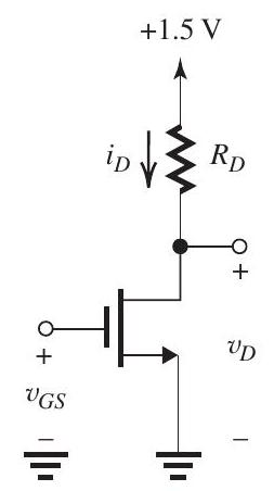
Figure 7.1.1
The NMOS transistor in the circuit in Fig. 7.1.1 has , and
(a) Find the value of that results in saturationmode operation with a dc current of . Neglect the Early effect.
(b) Find the value of that results in a dc drain voltage of .
(c) Find and at the dc operating point specified above. Assume .
(d) Find the open-circuit voltage gain .
(e) If a sinusoidal signal with peak amplitude is superimposed on the dc voltage , find the maximum allowable value of for which the transistor operates in saturation.
Question
Question
Question
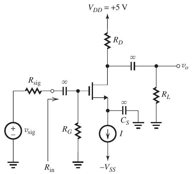
Figure 7.4.1
The MOSFET in the circuit of Fig. 7.4.1 has .
(a) Find the value of that causes the MOSFET to operate in saturation with an overdrive voltage of .
(b) What value of results in ?
(c) Find the value of .
(d) Find the value of given that .
(e) If is to be , find the value that must have. (f) For and , find the value of the overall voltage gain .
(g) What does the voltage gain become if is removed?
Question
Figure 7.5.1 (refer to Figure below)
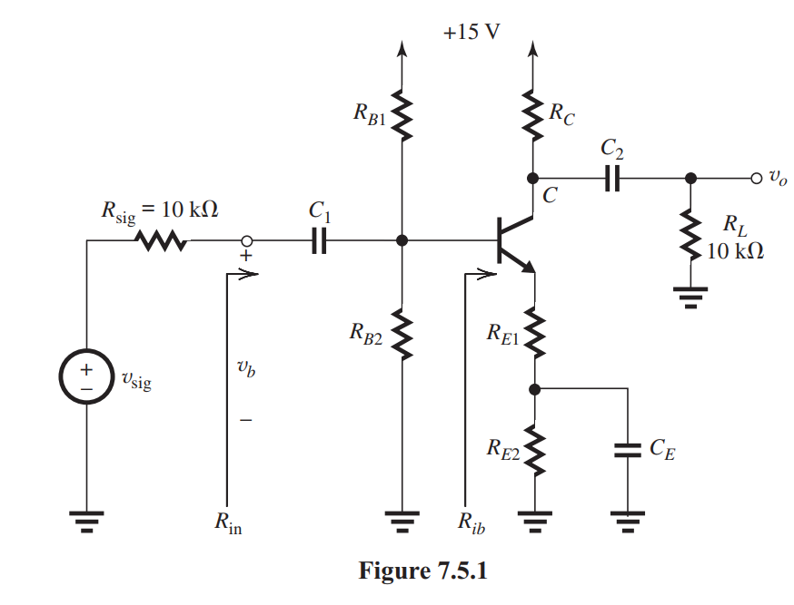
shows a capacitively coupled amplifier. In the following, assume operation at midband frequencies where the coupling and bypass capacitors behave as short circuits. The BJT has and the Early effect can be neglected.
(a) If the de voltage at the base is to be and the emitter current , find the required value of . Assume .
(b) If the input resistance at the base, , is to be , find the required value of and hence the value of .
(c) If the dc current in is to be , find the values of and .
(d) Find the value of that results in a de voltage of at the collector.
(e) Find the input resistance and the value of .
(f) Find the value of .
(g) Find the value of the overall voltage gain .
(h) If the peak amplitude of the signal between base and emitter is to be limited to , what are the corresponding amplitudes of , and ?
Question
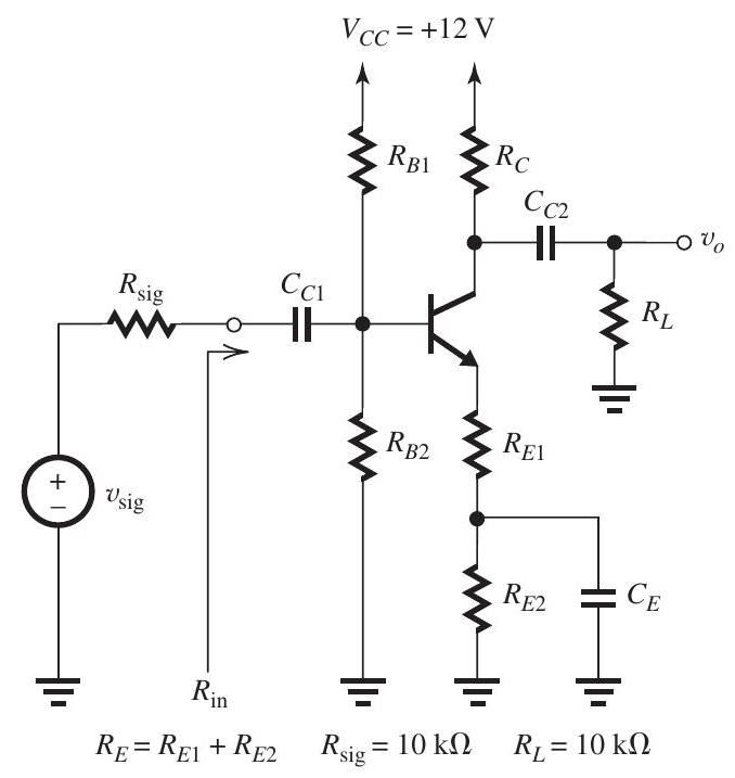
Figure 7.6.1
(a) Perform a dc bias design for the amplifier in Fig. 7.6.1. For this purpose, assume is very high and and neglect the Early effect. Design to obtain a dc base voltage of , a dc emitter current of , and a dc voltage at the collector that allows for signal swing at the collector with the minimum collector voltage no lower than . Use a de current in the base voltage divider of . What values are required for , and ?
(b) If the transistor has , find the actual values obtained for , and .
(c) What are the values of , and at the dc bias point.
(d) Assuming very large coupling and bypass capacitors, find the values of and that result in .
(e) Find the overall voltage gain .
(f) For , a sine wave with a peak amplitude, what is the peak amplitude required of the sine wave ? If this value is greater than , reduce to limit the peak amplitude of to . What is the resulting output voltage in this case?
Question
The transistor in the emitter follower of Fig. 7.7.1 (refer to Figure below)
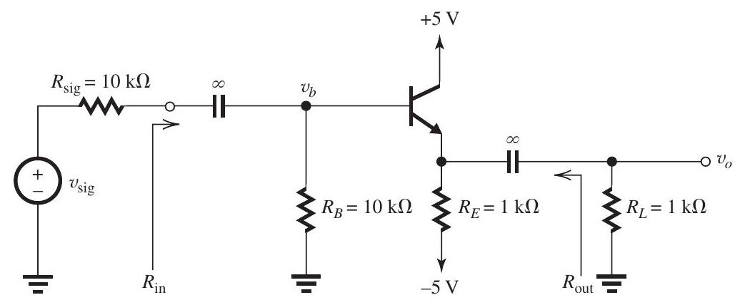
Figure 7.7.1
has . Assume and neglect the Early effect.
(a) Find the dc emitter current .
(b) Find the value of the emitter resistance .
(c) Find the input resistance .
(d) Find the voltage gain from signal source to the transistor base, .
(e) Find the voltage gain from transistor base to the output, .
(f) Find the overall voltage gain, .
(g) Find the output resistance .
Question
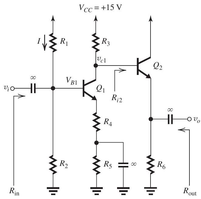
Figure 7.8.1
The transistors in the amplifier shown in Fig. 7.8.1
have , and negligible Early effect.
(a) Design the circuit to obtain the following dc operating parameters: , , and . Use . Find the values of , and . (b) Find the value of (and hence ) that results in .
(c) Find .
(d) Find the voltage gain .
(e) Find the voltage gain .
(f) Find the overall voltage gain .
(g) Find the output resistance .
(h) In order to minimize nonlinear distortion, it is required to keep the maximum signal across the base-emitter junction of each of and to . Under this constraint, what is the maximum peak-to-peak sine wave signal that can be obtained at the output?

Unlock Deck
Sign up to unlock the cards in this deck!
Unlock Deck
Unlock Deck
1/8
Play
Full screen (f)
Deck 3: Transistor Amplifiers
1
Figure 7.1.1
The NMOS transistor in the circuit in Fig. 7.1.1 has , and
(a) Find the value of that results in saturationmode operation with a dc current of . Neglect the Early effect.
(b) Find the value of that results in a dc drain voltage of .
(c) Find and at the dc operating point specified above. Assume .
(d) Find the open-circuit voltage gain .
(e) If a sinusoidal signal with peak amplitude is superimposed on the dc voltage , find the maximum allowable value of for which the transistor operates in saturation.
(a)
Figure 7.1.1
(b)
(c)
where
(d)
(e) At the edge of saturation,
Here,
Thus,
Figure 7.1.1
(b)
(c)
where
(d)
(e) At the edge of saturation,
Here,
Thus,
2
An NMOS transistor fabricated in a CMOS technology has and . The technology is specified to have , and .
(a) If the device is operated in saturation with an overdrive voltage of , find the required values of and , along with the resulting values of and . (b) If the gate width is doubled but the value of is maintained, what do the values of , and become?
(a) If the device is operated in saturation with an overdrive voltage of , find the required values of and , along with the resulting values of and . (b) If the gate width is doubled but the value of is maintained, what do the values of , and become?
(a) Saturation with ,
(b) If is doubled while is maintained, we see from Eq. (1) that doubles to
From
we see that doubles to
Finally, from
we see that is halved to
(b) If is doubled while is maintained, we see from Eq. (1) that doubles to
From
we see that doubles to
Finally, from
we see that is halved to
3
A CMOS technology is specified to have , and dc power supply of .
(a) Find the transconductance parameters and expressed in .
(b) Find the ratios of matched NMOS and PMOS transistors that exhibit resistance of when operated in the triode region with an overdrive voltage of . If twice-theminimum channel length is used, specify the width of the NMOS transistor and the PMOS transistor.
(c) If the devices in (b) are operated in saturation with , what drain current results? If for each transistor the source is connected to ground, what should the gate voltages be? In each case, specify the range of voltages permitted at the drain for saturation-mode operation to be maintained.
(d) If the drain currents in (c) are to be reduced by a factor of 4 , what should the overdrive voltage be? If instead of changing , the IC designer redesigns the widths of the transistors, what values would be required?
(e) If the devices described in (b) above are operated in saturation with , find the resulting value of .
(f) If an NMOS transistor as in (e) above is connected as a common-source amplifier with and , what dc voltage would appear at the drain? What small-signal voltage gain would be obtained?
(g) Recalculate the voltage gain in (f) taking into account channel-length modulation. Assume the
Early voltage for the process technology is specified as .
(a)
(b) For an NMOS transistor operating in a triode region,
For a matched PMOS transistor,
Thus,
(c)
For the NMOS transistor,
For the PMOS transistor,
Figure 7.3.1
From Fig. 7.3.1, we see that for the NMOS transistor to operate in saturation,
that is,
For the PMOS transistor to operate in saturation,
that is,
(d) Since is proportional to , the drain current can be reduced by a factor of 4 by reducing by a factor of 2 , that is, to . Alternatively, can be kept constant and reduced by a factor of 4 , resulting in
and
(e)
(f)
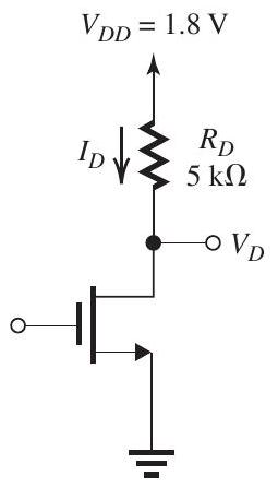
Figure 7.3.2
Refer to Fig. 7.3.2.
(b) For an NMOS transistor operating in a triode region,
For a matched PMOS transistor,
Thus,
(c)
For the NMOS transistor,
For the PMOS transistor,
Figure 7.3.1
From Fig. 7.3.1, we see that for the NMOS transistor to operate in saturation,
that is,
For the PMOS transistor to operate in saturation,
that is,
(d) Since is proportional to , the drain current can be reduced by a factor of 4 by reducing by a factor of 2 , that is, to . Alternatively, can be kept constant and reduced by a factor of 4 , resulting in
and
(e)
(f)
Figure 7.3.2
Refer to Fig. 7.3.2.
4
Figure 7.4.1
The MOSFET in the circuit of Fig. 7.4.1 has .
(a) Find the value of that causes the MOSFET to operate in saturation with an overdrive voltage of .
(b) What value of results in ?
(c) Find the value of .
(d) Find the value of given that .
(e) If is to be , find the value that must have. (f) For and , find the value of the overall voltage gain .
(g) What does the voltage gain become if is removed?
Unlock Deck
Unlock for access to all 8 flashcards in this deck.
Unlock Deck
k this deck
5
Figure 7.5.1 (refer to Figure below)
shows a capacitively coupled amplifier. In the following, assume operation at midband frequencies where the coupling and bypass capacitors behave as short circuits. The BJT has and the Early effect can be neglected.
(a) If the de voltage at the base is to be and the emitter current , find the required value of . Assume .
(b) If the input resistance at the base, , is to be , find the required value of and hence the value of .
(c) If the dc current in is to be , find the values of and .
(d) Find the value of that results in a de voltage of at the collector.
(e) Find the input resistance and the value of .
(f) Find the value of .
(g) Find the value of the overall voltage gain .
(h) If the peak amplitude of the signal between base and emitter is to be limited to , what are the corresponding amplitudes of , and ?
Unlock Deck
Unlock for access to all 8 flashcards in this deck.
Unlock Deck
k this deck
6
Figure 7.6.1
(a) Perform a dc bias design for the amplifier in Fig. 7.6.1. For this purpose, assume is very high and and neglect the Early effect. Design to obtain a dc base voltage of , a dc emitter current of , and a dc voltage at the collector that allows for signal swing at the collector with the minimum collector voltage no lower than . Use a de current in the base voltage divider of . What values are required for , and ?
(b) If the transistor has , find the actual values obtained for , and .
(c) What are the values of , and at the dc bias point.
(d) Assuming very large coupling and bypass capacitors, find the values of and that result in .
(e) Find the overall voltage gain .
(f) For , a sine wave with a peak amplitude, what is the peak amplitude required of the sine wave ? If this value is greater than , reduce to limit the peak amplitude of to . What is the resulting output voltage in this case?
Unlock Deck
Unlock for access to all 8 flashcards in this deck.
Unlock Deck
k this deck
7
The transistor in the emitter follower of Fig. 7.7.1 (refer to Figure below)
Figure 7.7.1
has . Assume and neglect the Early effect.
(a) Find the dc emitter current .
(b) Find the value of the emitter resistance .
(c) Find the input resistance .
(d) Find the voltage gain from signal source to the transistor base, .
(e) Find the voltage gain from transistor base to the output, .
(f) Find the overall voltage gain, .
(g) Find the output resistance .
Unlock Deck
Unlock for access to all 8 flashcards in this deck.
Unlock Deck
k this deck
8
Figure 7.8.1
The transistors in the amplifier shown in Fig. 7.8.1
have , and negligible Early effect.
(a) Design the circuit to obtain the following dc operating parameters: , , and . Use . Find the values of , and . (b) Find the value of (and hence ) that results in .
(c) Find .
(d) Find the voltage gain .
(e) Find the voltage gain .
(f) Find the overall voltage gain .
(g) Find the output resistance .
(h) In order to minimize nonlinear distortion, it is required to keep the maximum signal across the base-emitter junction of each of and to . Under this constraint, what is the maximum peak-to-peak sine wave signal that can be obtained at the output?
Unlock Deck
Unlock for access to all 8 flashcards in this deck.
Unlock Deck
k this deck
Unlock Deck
Unlock for access to all 8 flashcards in this deck.


