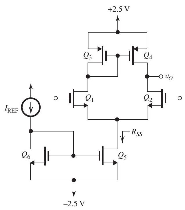
Solved

Figure 971
the Current-Mirror-Loaded CMOS Amplifier Shown in Fig 0.5μm0.5-\mu \mathrm{m}

Question 7

Essay

     Figure 9.7.1 The current-mirror-loaded CMOS amplifier shown in Fig. 9.7.1 is fabricated in a  0.5-\mu \mathrm{m}  technology for which  V_{t n}=-V_{t p}=0.5 \mathrm{~V},\left|V_{A}\right|=20 \mathrm{~V} , and  \mu_{n} C_{o x}=2 \mu_{p} C_{o x}=200 \mu \mathrm{A} / \mathrm{V}^{2} . Transistors  Q_{1}  and  Q_{2}  are matched,  Q_{3}  and  Q_{4}  are matched, and  Q_{5}  and  Q_{6}  are matched. The  (W / L)  ratios of all devices are selected so that all operate at the same  \left|V_{O V}\right| . (a) Starting from  \left|A_{d}\right|=g_{m 1}\left(r_{o 2} \| r_{o 4}\right)  and  \left|A_{c m}\right|=1 / 2 g_{m 3} R_{S S}  show that  \left|A_{d}\right|=\left|V_{A}\right| /\left|V_{O V}\right|  and  \mathrm{CMRR}=2\left(\left|V_{A}\right| /\left|V_{O V}\right|\right)^{2}  (b) To obtain a differential gain of  40 \mathrm{~V} / \mathrm{V} , find the overdrive voltage  \left|V_{O V}\right|  at which the transistors should be operated. Also, find the resulting CMRR in  \mathrm{dB} . (c) Using a reference current  I_{\mathrm{REF}}=200 \mu \mathrm{A} , find the  (W / L)  required for each of the six transistors. (d) With both input terminals grounded, what dc voltage occurs at the output (neglecting the Early effect)? Hence, compute the systematic input offset voltage. (e) Find the input common-mode range. (f) If the input differential signal is riding on an input common-mode voltage of  0 \mathrm{~V} , what is the maximum allowable output voltage swing in both directions? Hence, find the peak-to-peak amplitude of the largest sine-wave signal that can be applied between the two input terminals (without dc offset compensation).

Figure 9.7.1
The current-mirror-loaded CMOS amplifier shown in Fig. 9.7.1 is fabricated in a 0.5μm0.5-\mu \mathrm{m} technology for which Vtn=Vtp=0.5 V,VA=20 VV_{t n}=-V_{t p}=0.5 \mathrm{~V},\left|V_{A}\right|=20 \mathrm{~V} , and μnCox=2μpCox=200μA/V2\mu_{n} C_{o x}=2 \mu_{p} C_{o x}=200 \mu \mathrm{A} / \mathrm{V}^{2} . Transistors Q1Q_{1} and Q2Q_{2} are matched, Q3Q_{3} and Q4Q_{4} are matched, and Q5Q_{5} and Q6Q_{6} are matched. The (W/L)(W / L) ratios of all devices are selected so that all operate at the same VOV\left|V_{O V}\right| .
(a) Starting from
Ad=gm1(ro2ro4)\left|A_{d}\right|=g_{m 1}\left(r_{o 2} \| r_{o 4}\right)
and
Acm=1/2gm3RSS\left|A_{c m}\right|=1 / 2 g_{m 3} R_{S S}
show that
Ad=VA/VOV\left|A_{d}\right|=\left|V_{A}\right| /\left|V_{O V}\right|
and
CMRR=2(VA/VOV)2\mathrm{CMRR}=2\left(\left|V_{A}\right| /\left|V_{O V}\right|\right)^{2}
(b) To obtain a differential gain of 40 V/V40 \mathrm{~V} / \mathrm{V} , find the overdrive voltage VOV\left|V_{O V}\right| at which the transistors should be operated. Also, find the resulting CMRR in dB\mathrm{dB} .
(c) Using a reference current IREF=200μAI_{\mathrm{REF}}=200 \mu \mathrm{A} , find the (W/L)(W / L) required for each of the six transistors.
(d) With both input terminals grounded, what dc voltage occurs at the output (neglecting the Early effect)? Hence, compute the systematic input offset voltage.
(e) Find the input common-mode range.
(f) If the input differential signal is riding on an input common-mode voltage of 0 V0 \mathrm{~V} , what is the maximum allowable output voltage swing in both directions? Hence, find the peak-to-peak amplitude of the largest sine-wave signal that can be applied between the two input terminals (without dc offset compensation).

Correct Answer:

verifed

Verified

blured image

Figure 9.7.1
(a)
\[\begin{aligned}
g_ ...

View Answer

Unlock this answer now
Get Access to more Verified Answers free of charge

Related Questions

Unlock this Answer For Free Now!

View this answer and more for free by performing one of the following actions

qr-code

Scan the QR code to install the App and get 2 free unlocks

upload documents

Unlock quizzes for free by uploading documents