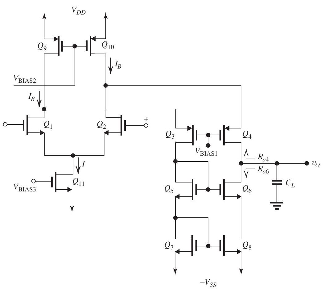
Figure 13.2.1
It is required to design the folded-cascode op amp shown in Fig. 13.2.1. Let and , and assume that for all transistors, . Design so that the power dissipated in the circuit (with no input signal applied) is , and so that each of and is operating at a current four times that at which each of and is operating. Also, design so that all transistors operate at .
(a) Show that the current drawn from each of the two power supplies is , and hence find and that result in the circuit operating at its specified power dissipation.
(b) Find the dc current at which each of to is operating. Present your results in a table.
(c) Find the input common-mode range.
(d) Find the required values of , and that result in the maximum allowable value of to be as high as possible.
(e) Find the allowable range of .
(f) Find the overall transconductance .
(g) Find the output resistance .
(h) Find the low-frequency voltage gain.
(i) If the amplifier at its output is modeled by a controlled current-source (where is the differential input voltage) feeding the output resistance and the total capacitance at the output node , find the value of that results in the amplifier having a unity-gain bandwidth of . Assume that the dominant pole is that formed at the output.
Correct Answer:
Verified

