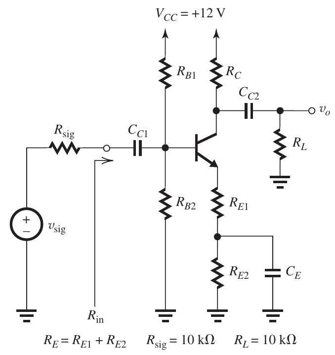
Figure 7.6.1
(a) Perform a dc bias design for the amplifier in Fig. 7.6.1. For this purpose, assume is very high and and neglect the Early effect. Design to obtain a dc base voltage of , a dc emitter current of , and a dc voltage at the collector that allows for signal swing at the collector with the minimum collector voltage no lower than . Use a de current in the base voltage divider of . What values are required for , and ?
(b) If the transistor has , find the actual values obtained for , and .
(c) What are the values of , and at the dc bias point.
(d) Assuming very large coupling and bypass capacitors, find the values of and that result in .
(e) Find the overall voltage gain .
(f) For , a sine wave with a peak amplitude, what is the peak amplitude required of the sine wave ? If this value is greater than , reduce to limit the peak amplitude of to . What is the resulting output voltage in this case?
Correct Answer:
Verified
Figure 7.6.1
Figure 7.6.2
(a) Refe...
View Answer
Unlock this answer now
Get Access to more Verified Answers free of charge

