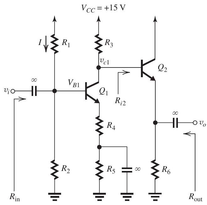
Solved

Figure 781
the Transistors in the Amplifier Shown in Fig β=100,VBE=0.7 V\beta=100, V_{B E}=0.7 \mathrm{~V}

Question 8

Essay

    Figure 7.8.1 The transistors in the amplifier shown in Fig. 7.8.1 have  \beta=100, V_{B E}=0.7 \mathrm{~V} , and negligible Early effect. (a) Design the circuit to obtain the following dc operating parameters:  V_{B 1}=+3 \mathrm{~V}, I_{E 1}=1 \mathrm{~mA} ,  V_{E 2}=+4 \mathrm{~V} , and  I_{E 2}=4 \mathrm{~mA} . Use  I=0.1 \mathrm{~mA} . Find the values of  R_{1}, R_{2}, R_{3},\left(R_{4}+R_{5}\right) , and  R_{6} . (b) Find the value of  R_{4}  (and hence  R_{5}  ) that results in  R_{\text {in }}=10 \mathrm{k} \Omega . (c) Find  R_{i 2} . (d) Find the voltage gain  v_{c 1} / v_{i} . (e) Find the voltage gain  v_{O} / v_{c 1} . (f) Find the overall voltage gain  v_{o} / v_{i} . (g) Find the output resistance  R_{\text {out }} . (h) In order to minimize nonlinear distortion, it is required to keep the maximum signal across the base-emitter junction of each of  Q_{1}  and  Q_{2}  to  5 \mathrm{mV} . Under this constraint, what is the maximum peak-to-peak sine wave signal that can be obtained at the output?
Figure 7.8.1
The transistors in the amplifier shown in Fig. 7.8.1
have β=100,VBE=0.7 V\beta=100, V_{B E}=0.7 \mathrm{~V} , and negligible Early effect.
(a) Design the circuit to obtain the following dc operating parameters: VB1=+3 V,IE1=1 mAV_{B 1}=+3 \mathrm{~V}, I_{E 1}=1 \mathrm{~mA} , VE2=+4 VV_{E 2}=+4 \mathrm{~V} , and IE2=4 mAI_{E 2}=4 \mathrm{~mA} . Use I=0.1 mAI=0.1 \mathrm{~mA} . Find the values of R1,R2,R3,(R4+R5)R_{1}, R_{2}, R_{3},\left(R_{4}+R_{5}\right) , and R6R_{6} . (b) Find the value of R4R_{4} (and hence R5R_{5} ) that results in Rin =10kΩR_{\text {in }}=10 \mathrm{k} \Omega .
(c) Find Ri2R_{i 2} .
(d) Find the voltage gain vc1/viv_{c 1} / v_{i} .
(e) Find the voltage gain vO/vc1v_{O} / v_{c 1} .
(f) Find the overall voltage gain vo/viv_{o} / v_{i} .
(g) Find the output resistance Rout R_{\text {out }} .
(h) In order to minimize nonlinear distortion, it is required to keep the maximum signal across the base-emitter junction of each of Q1Q_{1} and Q2Q_{2} to 5mV5 \mathrm{mV} . Under this constraint, what is the maximum peak-to-peak sine wave signal that can be obtained at the output?

Correct Answer:

verifed

Verified

blured image
blured image

(a) Refer to Fig. 7.8.2.
\[\begin{ ...

View Answer

Unlock this answer now
Get Access to more Verified Answers free of charge

Related Questions

Unlock this Answer For Free Now!

View this answer and more for free by performing one of the following actions

qr-code

Scan the QR code to install the App and get 2 free unlocks

upload documents

Unlock quizzes for free by uploading documents